Group III nitride compound semiconductor devices and method for fabricating the same

a technology of nitride compound semiconductors and compound semiconductors, which is applied in the direction of semiconductor lasers, semiconductor laser structural details, lasers, etc., can solve the problems of poor device characteristics, low mobility of semiconductor devices, and device problems of unsatisfactory device characteristics, so as to improve service life and mobility. , the effect of improving the ld threshold valu

Inactive Publication Date: 2006-03-23
TOYODA GOSEI CO LTD
View PDF24 Cites 95 Cited by
  • Summary
  • Abstract
  • Description
  • Claims
  • Application Information

AI Technical Summary

Benefits of technology

[0006] The aforementioned dislocations will next be described with reference to a sketch of FIG. 18. FIG. 18 shows a substrate 91, a buffer layer 92 formed thereon, and a Group III nitride compound semiconductor layer 93 further formed thereon. Conventionally, the substrate 91 is formed of sapphire or a similar substance and the buffer layer 92 is formed of aluminum nitride (AlN) or a similar substance. The buffer layer 92 formed of aluminum nitride (AlN) is provided so as to relax misfit between the sapphire substrate 91 and the Group III nitride compound semiconductor layer 93. However, generation of dislocations is not reduced to zero. Threading dislocations 901 propagate upward (in a vertical direction with respect to the substrate surface) from dislocation initiating points 900, penetrating the buffer layer 92 and the Group III nitride compound semiconductor layer 93. When a semiconductor device is fabricated by stacking various types of Group III nitride compound semiconductors of interest on the Group III nitride compound semiconductor layer 93, threading dislocations further propagate upward, through the semiconductor device, from dislocation arrival points 902 on the surface of the Group III nitride compound semiconductor layer 93. Thus, according to conventional techniques, problematic propagation of dislocations cannot be prevented during formation of Group III nitride compound semiconductor layers.
[0024] When the rate that the Group III nitride compound semiconductor 31, which epitaxially grows in lateral direction from the buffer layer 21 formed on the upper surface of the post or mesa, coalescences to the lateral epitaxial growth layer starting from the upper surface of the post facing to each other is faster than the rate that the Group III nitride compound semiconductor 32, which epitaxially grows in vertical direction from the buffer layer 22 formed on the bottom surface of the trench, grows to the upper layer of the post, threading dislocations propagated from the buffer layer 22 formed on the bottom layer of the trench is remarkably suppressed in the upper portion of the thus-buried Group III nitride compound semiconductor 31, to thereby provide a crystal region of remarkably high quality. In this case, as shown in FIG. 1(d), the growth front of the Group III nitride compound semiconductor 32 which is grown from the buffer layer 22 formed on the bottom portion of the trench serving as a seed for crystal growth is not exposed at the surface but remains as cavities. And over the cavities, growth fronts of the Group III nitride compound semiconductor 31 grown from the buffer layer, formed on the upper layer of the post of both sides and serving as seeds for crystal growth, coalesce. The propagation of threading dislocations from the buffer layer 22 can be prevented at the cavities.
[0029] As shown in FIG. 5(a), the buffer layer 2 is formed on the substrate 1. Then as shown in FIG. 5(b), portions of the buffer layer 2 and the substrate 1 are removed, so as to provide trenches / posts. As shown in FIG. 5(c), a Group III nitride compound layer 31 is epitaxially grown, vertically and laterally, with mainly the buffer layer 2 serving as a seed for crystal growth. FIG. 5(c) illustrates the Group III nitride compound semiconductor 32 growing epitaxially from the bottom surfaces and sidewalls of the trenches / posts. When the rate that the Group III nitride compound semiconductor 31, which epitaxially grows in lateral direction from the buffer layer 2 formed on the upper surface of the post, coalescences to the lateral epitaxial growth front starting from the upper surface of the post facing to each other is faster than the rate that the Group III nitride compound semiconductor 32, which epitaxially grows in vertical direction from the buffer layer 2 formed on the bottom surface and the sidewall of the trench, grows to the upper layer of the post, threading dislocations propagated from the bottom layer of the trench is remarkably suppressed in the upper portion of the thus-buried Group III nitride compound semiconductor 31, to thereby provide a crystal region of remarkably high quality. In this case, as shown in FIG. 5(d), the growth layer of the Group III nitride compound semiconductor 32 which is grown from the buffer layer 2 formed on the bottom portion of the trench serving as a seed for crystal growth is not exposed at the surface but remains as cavities. And over the cavities, growth fronts of the Group III nitride compound semiconductor 31 grown from the buffer layer 2, formed on the upper layer of the post of both sides and serving as seeds for crystal growth, coalesce. The propagation of threading dislocations from the buffer layer 2 can be prevented at the cavities.
[0037] By forming a device element as an upper layer on a portion of a Group III nitride compound semiconductor layer that is formed through lateral epitaxial growth through the above step, there can be provided a semiconductor device having a layer containing few defects and endowed with high mobility (eleventh feature).
[0038] By stacking, as an upper layer, a light-emitting element on a portion of a Group III nitride compound semiconductor layer that is formed through the above step, there can be provided a light-emitting device endowed with improved service life and improved LD threshold value (twelfth feature).

Problems solved by technology

However, when a Group III nitride compound semiconductor is formed on a sapphire substrate, misfit-induced dislocations occur due to difference between the lattice constant of sapphire and that of the semiconductor, resulting in poor device characteristics.
Misfit-induced dislocations are threading dislocations which penetrate semiconductor layers in a longitudinal direction (i.e., in a direction vertical to the surface of the substrate), and Group III nitride compound semiconductors are accompanied by the problem that dislocations in amounts of approximately 109 cm−2 propagate therethrough.
When such a semiconductor is incorporated in, for example, a light-emitting device, the device poses problems of unsatisfactory device characteristics in terms of threshold current of an LD, service life of an LED or LD, etc.
On the other hand, when a Group III nitride compound semiconductor is incorporated in any of other types of semiconductor devices, because electrons are scattered due to defects in the Group III nitride compound semiconductor, the semiconductor device comes to have low mobility.
These problems are not solved even when another type of substrate is employed.
Thus, according to conventional techniques, problematic propagation of dislocations cannot be prevented during formation of Group III nitride compound semiconductor layers.

Method used


Image

  • Group III nitride compound semiconductor devices and method for fabricating the same
  • Group III nitride compound semiconductor devices and method for fabricating the same
  • Group III nitride compound semiconductor devices and method for fabricating the same

Examples


first embodiment

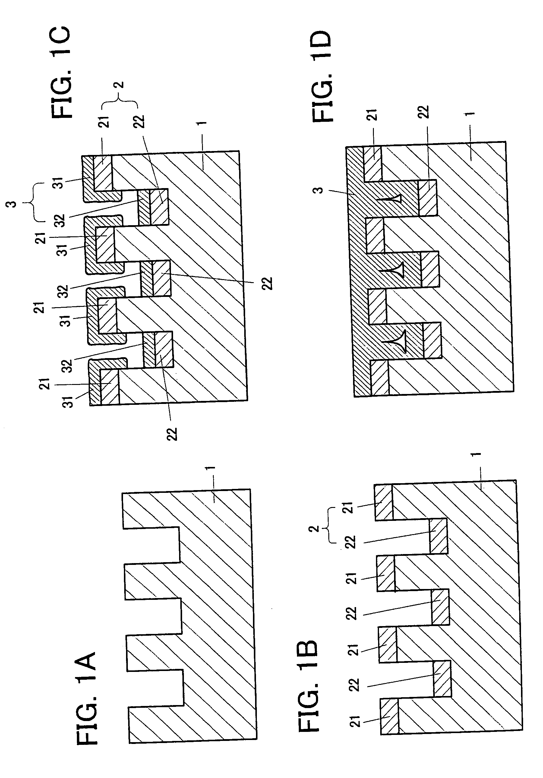
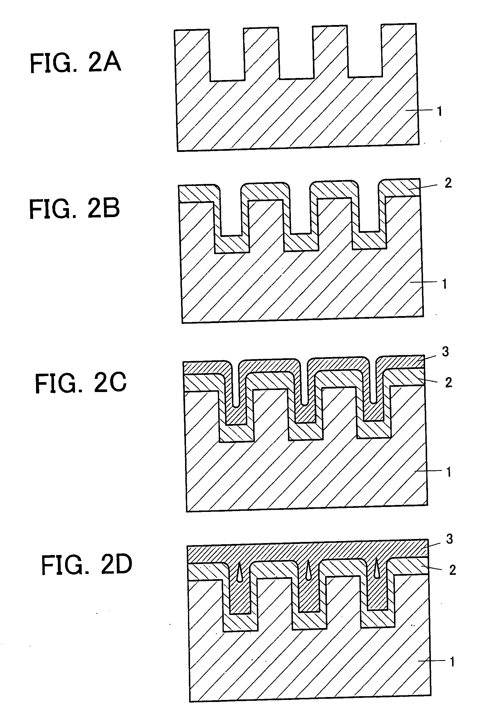
[0081] A monocrystalline sapphire substrate 1 was prepared such that the a-plane thereof cleaned through organic cleaning and heat treatment serves as the main surface thereof. By carrying out dicing, trenches each having a width of 10 μm and a depth of 10 μm were formed at 10 μm of intervals in a stripe pattern. Next, temperature was set to 400° C., and H2 (10 L / min), NH3 (5 L / min), and TMA (20 μmol / min) were supplied for approximately 3 minutes to thereby form, on the sapphire substrate 1, a buffer layer 2 of AlN having a thickness of approximately 40 nm. The buffer layer 2 was formed mainly on the upper surface and the bottom surface of the trenches of the substrate 1.

[0082] Next, while the temperature of the sapphire substrate 1 was maintained at 1150° C., H2 (20 L / min), NH3 (10 L / min), and TMG (5 μmol / min) were introduced to thereby form a GaN layer 3 through vertical and lateral epitaxial growth. At this time, lateral epitaxial growth from the buffer layer 21, which was mainl...

second embodiment

[0083] A monocrystalline sapphire substrate 1 was prepared such that the a-plane thereof cleaned through organic cleaning and heat treatment serves as the main surface thereof. Temperature was dropped to 400° C., and H2 (10 L / min), NH3 (5 L / min), and TMA (20 μmol / min) were supplied for approximately 3 minutes to thereby form, on the sapphire substrate 1, an AlN layer (first buffer layer) 2 having a thickness of approximately 40 nm. Next, by carrying out dicing, trenches each having a width of 10 μm and a depth of 10 μm were formed at 10 μm of intervals in a stripe pattern. The buffer layer 2 remained only on the upper surface of posts of the substrate 1 (FIG. 5(b)).

[0084] Next, while the temperature of the sapphire substrate 1 was maintained at 1150° C., H2 (20 L / min), NH3 (10 L / min), and TMG (5 μmol / min) were introduced to thereby form a GaN layer 3 was formed through vertical and lateral epitaxial growth. At this time, lateral epitaxial growth from the buffer layer 2, which was m...

third embodiment

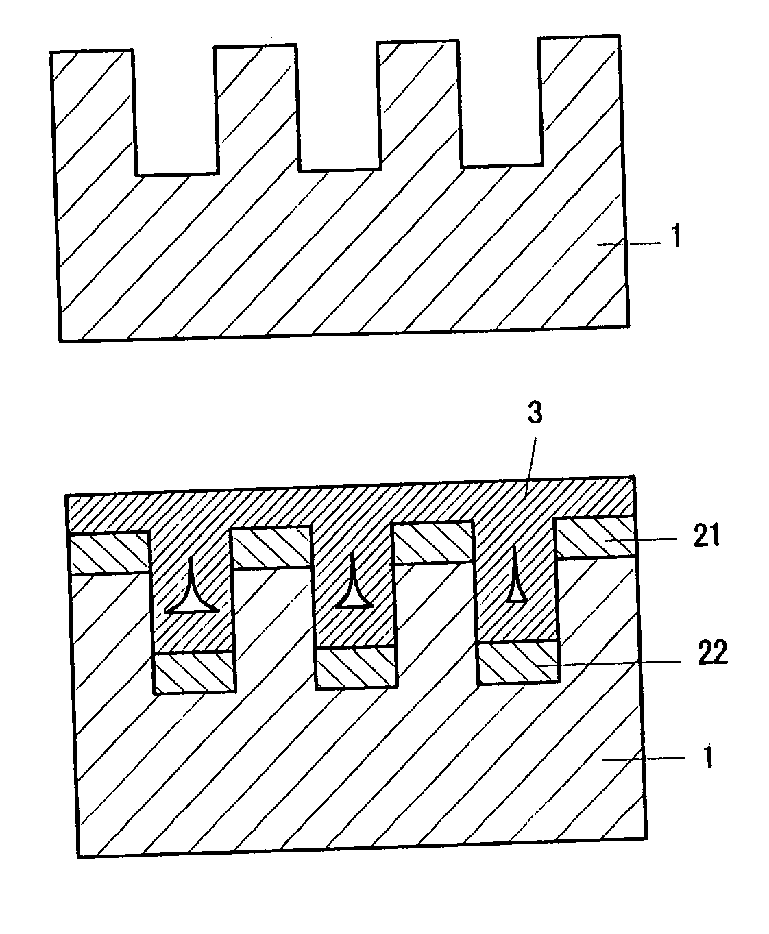
[0085] A monocrystalline sapphire substrate 1 was prepared such that the a-plane thereof cleaned through organic cleaning and heat treatment serves as the main surface thereof. Then the surface of the substrate 1 was selectively dry-etched in a short time by reactive ion beam etching (RIE) to have stripe-shaped ruggedness each having a width of 10 μm at intervals of 10 μm. Next, while the temperature of the sapphire substrate 1 was maintained at 400° C., H2 (10 L / min), NH3 (5 L / min), and TMA (20 μmol / min) were introduced for 3 minutes to thereby form an AlN buffer layer 2 having a thickness of about 40 nm. The surface morphology of the rugged portion 22 was different from that of the smooth portion 21 of the buffer layer 2 (FIG. 7(b)).

[0086] Next, while the temperature of the substrate 1 was maintained at 1150° C., H2 (20 L / min), NH3 (10 L / min), and TMA (5 μmol / min) were introduced to thereby form a GaN layer 3 through vertical and lateral epitaxial growth. At this time, mainly the...


PUM

PropertyMeasurementUnit
thicknessaaaaaaaaaa
thicknessaaaaaaaaaa
thicknessaaaaaaaaaa

Abstract

A sapphire substrate 1 is etched so that each trench has a width of 10 μm and a depth of 10 μm were formed at 10 μm of intervals in a stripe pattern. Next, an AlN buffer layer 2 having a thickness of approximately 40 nm is formed mainly on the upper surface and the bottom surface of the trenches of the substrate 1. Then a GaN layer 3 is formed through vertical and lateral epitaxial growth. At this time, lateral epitaxial growth of the buffer layer 21, which was mainly formed on the upper surface of the trenches, filled the trenches and thus establishing a flat top surface. The portions of the GaN layer 3 formed above the top surfaces of the mesas having a depth of 10 μm exhibited significant suppression of threading dislocation in contrast to the portions formed above the bottoms of the trenches.

Description

[0001] The present application is a Divisional Application of U.S. patent application Ser. No. 10 / 221,528, filed on Mar. 18, 2003.TECHNICAL FIELD [0002] The present invention relates to a method for fabricating Group III nitride compound semiconductors. More particularly, the present invention relates to a method for fabricating Group III nitride compound semiconductors employing epitaxial lateral overgrowth (ELO), Group III nitride compound semiconductor devices, and to Group III nitride compound semiconductor substrates. The Group III nitride compound semiconductors are generally represented by AlxGayIn1-x-yN (wherein 0≦x≦1, 0≦y≦1, and 0≦x+y≦1), and examples thereof include binary semiconductors such as AlN, GaN, and InN; ternary semiconductors such as AlxGa1-xN, AlxIn1-xN, and GaxIn1-xN (wherein 0<x<1); and quaternary semiconductors such as AlxGayIn1-x-yN (wherein 0<x<1, 0<y<1, and 0<x+y<1). [0003] In the present specification, unless otherwise specified, ...

Claims


Application Information

Patent Timeline
Patent Type & Authority Applications(United States)
IPC IPC(8): H01L33/00H01L31/12H01L27/15H01L29/26H01L21/20H01L21/205H01L33/06H01L33/12H01L33/32H01L33/34H01S5/02H01S5/323H01S5/343
CPCH01L21/0242H01L21/02458H01L21/0254H01L21/0262H01L21/02639H01S2304/12H01L21/0265H01L33/007H01L33/025H01S5/0213H01S5/32341H01L21/02647
Inventor TEZEN, YUTA
Owner TOYODA GOSEI CO LTD
Why Eureka
Try Eureka