Light source

a light source and light source technology, applied in semiconductor lasers, process and machine control, instruments, etc., can solve the problems of small light output amplitude (difference between light output pb>1/b>, light output pb>2/b>, level, etc., and achieve the effect of reducing the fall time and large light output amplitud

Active Publication Date: 2006-03-23
TOYODA GOSEI CO LTD
View PDF2 Cites 5 Cited by
  • Summary
  • Abstract
  • Description
  • Claims
  • Application Information

AI Technical Summary

Benefits of technology

[0025] The light source according to the invention can ensure

Problems solved by technology

However, the technique of JP-A-2003-163377 has a problem in that a light output amplitude (difference between the light output P1 when the light emitting diode is applied with the voltage at high level

Method used


Image

  • Light source
  • Light source
  • Light source

Examples


embodiments

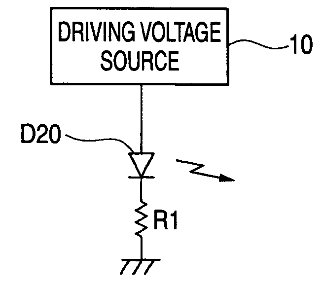
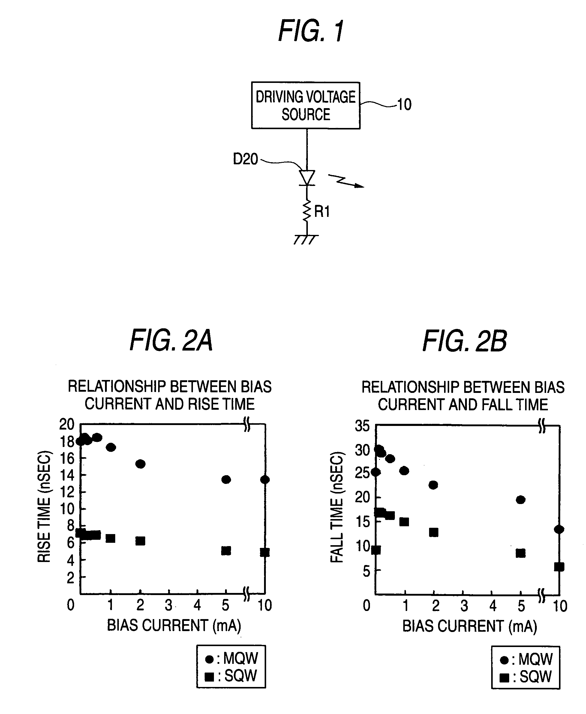
[0035] As illustrated in FIG. 1, a light source of this embodiment comprises a light emitting diode D20 made of a GaN (gallium nitride) based compound in single quantum well structure (hereinafter, abbreviated as SQW), and a driving voltage source 10 for applying a pulse voltage to the light emitting diode. The driving voltage source 10 applies a rectangular pulse voltage to the light emitting diode D20 based on digital data. The light emitting diode D20 has a cathode grounded through a resistor R1. SQW means that a light emitting diode comprises only one set of unit laminate structure comprised of a pair of cladding layers and an active layer sandwiched therebetween. The SQW light emitting diode D20 of this embodiment comprises only one of the laminate structure. The light emitting diode D20 of this embodiment is not limited in the shape and the like of the cladding layers or active layers, and can utilize any type of an edge emitting type or a surface emitting type. The light outp...


PUM


Abstract

A light source comprising a light emitting diode comprising a GaN-based compound and having a single quantum well structure, and a driving voltage source for applying a pulse voltage to the light emitting diode, wherein a voltage at a low level of the pulse voltage is set to a voltage lower than a voltage at which a fall time of the light emitting diode is made the longest.

Description

[0001] This application is based on Japanese Patent Application No. 2004-269687, which is incorporated herein by reference. BACKGROUND OF THE INVENTION [0002] 1. Field of the Invention [0003] The present invention relates to a light source which blinks at high rates. Particularly, the invention relates to a light source which can blink at a rate high enough to be utilized for optical communication. [0004] 2. Description of the Related Art [0005] There exist a large number of situations in which an optical communication system is desired to be built in a relatively short distance and to transmit a large amount of information. Investigations are now under progress for building an optical communication system in such situations using plastic optical fibers (hereinafter called the “POF”) at a low cost. [0006] In optical communication systems which utilize the POF or the like, an attempt has been made to utilize light emitting diodes made of group III-V compounds. For example, researches...

Claims


Application Information

Patent Timeline
IPC IPC(8): H05B41/36H01L33/00H01L33/06H01L33/32
CPCB82Y20/00H01S5/34333Y02B20/346H05B33/0845H05B33/0818H05B45/10Y02B20/30
Inventor KATO, SATORUKACHI, TETSUTOMITA, KAZUYOSHIITO, HIROSHIKOJIMA, MASANORI
Owner TOYODA GOSEI CO LTD
Why Eureka
Try Eureka