Switched-capacitor circuit and pipelined a/d converter

a technology of switching capacitor and circuit, which is applied in the direction of analogue/digital conversion, electrical analogy stores, instruments, etc., can solve the problems of poor signal-to-noise ratio (snr), relatively low operating speed of the circuit, and large power consumption of the amplifier, so as to achieve control signal and easy generation

Inactive Publication Date: 2006-03-23
FUJITSU LTD
View PDF10 Cites 9 Cited by
  • Summary
  • Abstract
  • Description
  • Claims
  • Application Information

AI Technical Summary

Benefits of technology

[0019] In a preferable example of the second aspect of the present invention, a switch control circuit of the pipelined A / D converter generates the control signal for turning off / on the switch circuit, according to a bit value outputted by a sub A / D converter connected to an input of the switched-capacitor circuit. Therefore, the control signal can be easily generated by using an output of the sub A / D converter.

Problems solved by technology

In conventional switched-capacitor circuits disclosed in the aforesaid patent document and so on, a feedback gain from an output to an input of an amplifier is as small as ½. Therefore, there has been a problem that power consumption of the amplifier becomes relatively large.
There has been a problem that reducing power consumption results in a relatively low operating speed of the circuit.
There has been another problem of a poor signal-to-noise ratio (SNR) since equivalent input noise of the amplifier is amplified twofold.

Method used


Image

  • Switched-capacitor circuit and pipelined a/d converter
  • Switched-capacitor circuit and pipelined a/d converter
  • Switched-capacitor circuit and pipelined a/d converter

Examples


first embodiment

[0056]FIG. 1 to FIG. 8 show the switched-capacitor circuit and the pipelined A / D converter of the present invention.

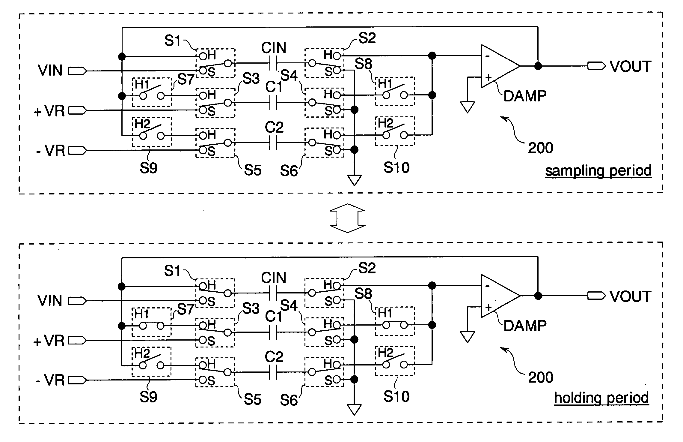
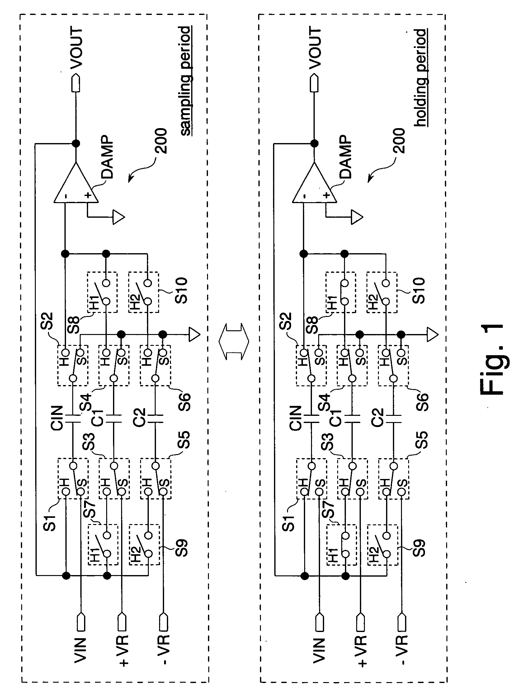
[0057]FIG. 1 shows details of a switched-capacitor circuit 200. Here, an input voltage VIN and an output voltage VOUT represent an input voltage and an output voltage of the switched-capacitor circuit 200. The switched-capacitor circuit 200 has an input capacitor CIN, a first and a second reference capacitor C1, C2, a switch circuit constituted of switches S1 to S10, and a differential amplifier DAMP. Capacitances of the capacitors CIN, C1, C2 are set to be equal to one another. Each of the switches S1 to S10 is constituted of an nMOS transistor, a pMOS transistor, or a CMOS transmission gate that turns on / off according to a gate voltage. “S” and “H” of the switches S1 to S6 represent switched-on sides when a high-level sampling signal S and a high-level holding signal H are received. “H1” of the switches S7, S8 represents that they turn on when receiving a high-level ...

fifth embodiment

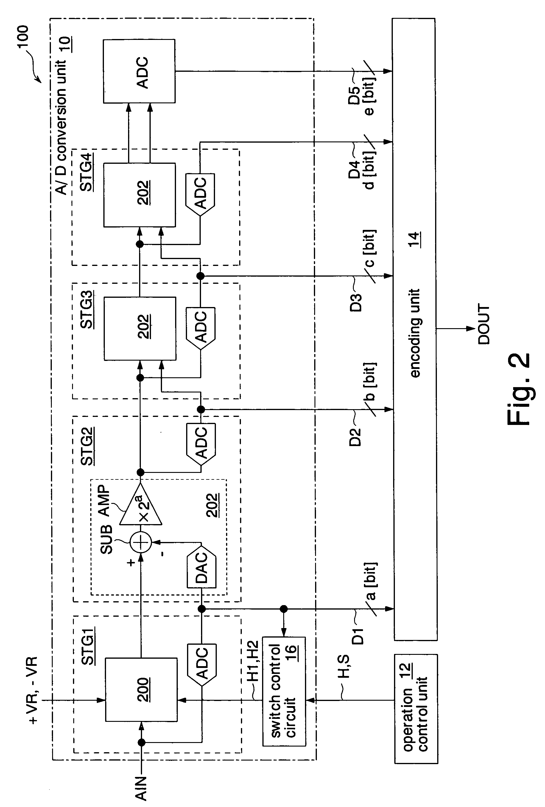
[0093] In the switched-capacitor circuit 200E, each of capacitors CIN, C1, C2 makes a pair with a sub-capacitor. Switches connecting the capacitors CIN, C1, C2 to voltage lines VIN, +VR, −VR, a ground voltage line, and a differential amplifier DAMP are formed to correspond to the sub-capacitors respectively. In this embodiment, each of stages STG1 to STG4 (see FIG. 2) of the pipelined A / D converter 100E determines 1.5 bits as in the

[0094] The switched-capacitor circuit 200E is controlled by a switch control circuit 16 (see FIG. 2) and switches the state of switches A, B, C, D to the state shown in the row of “+VR” in the drawing when a sub A / D converter ADC on a preceding stage outputs a digital value “11” (indicating a logical value “1”). An output voltage VOUT at this time is represented by an expression (11) (the same value as that of the expression (8)). Similarly, when the sub A / D converter ADC on the preceding stage outputs a digital value “01” (indicating a logical value “ind...


PUM


Abstract

An input capacitor and a plurality of reference capacitors sample an input voltage and reference voltages in a first period. A switch circuit connects the input capacitor and one of the reference capacitors between an output and an input of an amplifier in a second period. This mechanism causes a feedback gain to be “1” in the second period. Therefore, it is possible to reduce power consumption and noise.

Description

CROSS-REFERENCE TO RELATED APPLICATIONS [0001] This application is based upon and claims the benefit of priority from Japanese Patent Application No. 2004-271766, filed on Sep. 17, 2004, the entire contents of which are incorporated herein by reference. BACKGROUND OF THE INVENTION [0002] 1. Field of the Invention [0003] The present invention relates to a switched-capacitor circuit and a pipelined A / D converter configured by using the switched-capacitor circuit. [0004] 2. Description of the Related Art [0005] A pipelined A / D converter is well-known as a high-speed A / D converter with high resolution. [0006] Further, a switched-capacitor circuit is in wide use in order to enable the pipelined A / D converter to perform a series of signal processing with a simple circuit and with high accuracy. An example of the switched-capacitor circuit of this kind is disclosed in Japanese Unexamined Patent Application Publication No. 2000-13189. [0007] In conventional switched-capacitor circuits discl...

Claims


Application Information

Patent Timeline
Patent Type & Authority Applications(United States)
IPC IPC(8): H03M1/12
CPCG11C27/024G11C27/026H03M1/442H03M1/167H03M1/0695H03M1/44
Inventor YOSHIOKA, MASATOKUDO, MASAHIRO
Owner FUJITSU LTD
Why Eureka
Try Eureka