Method and apparatus for a low parasitic capacitance butt-joined passive waveguide connected to an active structure

Inactive Publication Date: 2006-03-23
AVAGO TECH INT SALES PTE LTD
View PDF6 Cites 3 Cited by
  • Summary
  • Abstract
  • Description
  • Claims
  • Application Information

AI Technical Summary

Benefits of technology

[0003] In accordance with the invention, passive Q waveguides are butt-joined to active EA modulators with low parasitic capacitance. While passive-Q waveguide core thickness is still important for minimizing mode mis

Problems solved by technology

However, when attempting to make a low parasitic electro-absorption (EA) modulator with passive waveguide there is an optimization problem because the parasitic capacitance value is determined by the thickness of passive Q-

Method used


Image

  • Method and apparatus for a low parasitic capacitance butt-joined passive waveguide connected to an active structure
  • Method and apparatus for a low parasitic capacitance butt-joined passive waveguide connected to an active structure
  • Method and apparatus for a low parasitic capacitance butt-joined passive waveguide connected to an active structure

Examples


Example

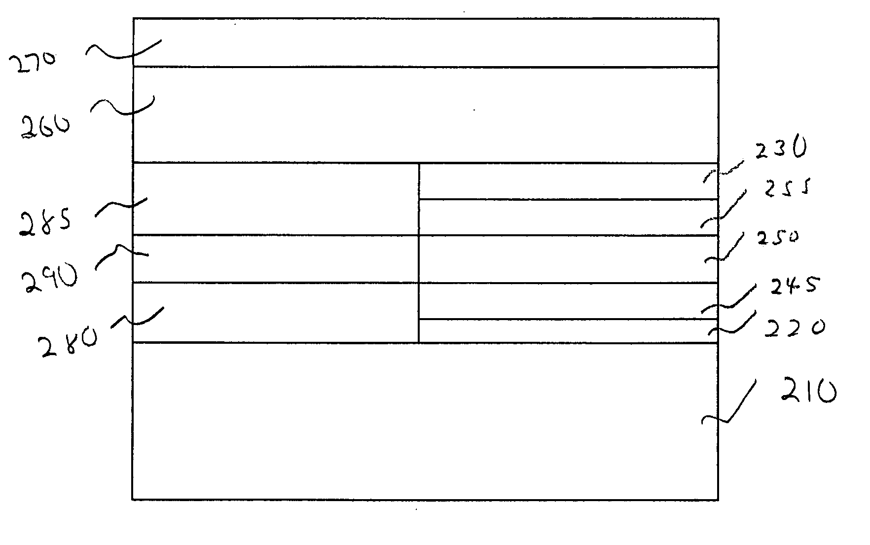
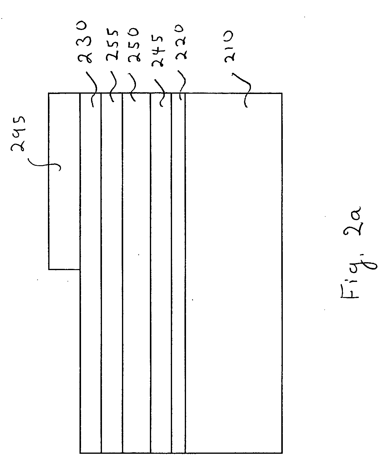
[0006]FIG. 2a shows an embodiment in accordance with the invention. On n-InP base wafer 210, active region 250 along with SCH layers 245 and 255 are grown using MOVCD (metal organic chemical vapor deposition) along with p-InP cladding layer 230 which is typically thicker, about 0.3 μm to 0.5 μm, than prior art p-InP cladding layer 130. SCH layers 245 and 255 typically have about a 1.15 μm bandgap. Typical growth parameters are a growth temperature of about 670° C., a growth pressure of about 76 torr, a V / III ratio of about 200 and a growth rate that is typically about 280 angstroms per minute. More details regarding active EA modulator structure 299 may be found in the patent application “Semiconductor Quantum Well Devices and Method of Making Same” filed Jun. 14, 2004, Ser. No. 10 / 867,037 and incorporated herein by reference.

[0007] SiO2 / Si3N4 mask 295 is then defined over part of p-InP layer 230. FIG. 2b shows etching, using for example, dry Cl and Ar RIE (reactive ion etching) an...


PUM

PropertyMeasurementUnit
Thicknessaaaaaaaaaa
Structureaaaaaaaaaa
Capacitanceaaaaaaaaaa

Abstract

Undoped layers are introduced in the passive waveguide section of a butt-joined passive waveguide connected to an active structure. This reduces the parasitic capacitance of the structure.

Description

BACKGROUND [0001] Typical methods to fabricate a butt-joined passive waveguide structure involves etching past the active region of the active device to grow the desired waveguide. FIG. 1 shows typical active passive butt joint structure 100. On n-InP base wafer 110, active region 150 is surrounded by separate confinement heterostructure (SCH) layers 145 and 155. P-InP cladding layer 130 and n-InP cladding layer 120 border on SCH layers 155 and 145, respectively. Passive Q-waveguide core 190 is sandwiched between n-InP layer 180 and p-InP layer 185. P-InP layer 160 serves as a cladding layer and p(+)-InGaAs layer 170 serves as a contact layer. To minimize mode mismatch losses at the interface between active region 150 and passive Q-waveguide core 190, the position and composition of passive Q-waveguide core 190 are appropriately selected. The presence of n-InP layer 180 and p-InP layer 185 on either side of passive Q-waveguide core 190 implies that the parasitic capacitance at the i...

Claims


Application Information

Patent Timeline
IPC IPC(8): G02B6/10
CPCG02B6/12004G02B6/42G02B6/26
Inventor RANGANATH, TIRUMALA R.ZHU, JINTIAN
Owner AVAGO TECH INT SALES PTE LTD
Why Eureka
Try Eureka