Method of making a microelectronic and/or optoelectronic circuitry sheet

a technology of optoelectronic circuitry and microelectronics, applied in the field of microelectronics and optoelectronic circuitry sheets, can solve the problems of limited success in attempts, significant manufacturing and engineering challenges, and limit the maximum temperature that may be used during the manufacturing of the end produ

Inactive Publication Date: 2006-03-23
VERSATILIS
View PDF46 Cites 238 Cited by
  • Summary
  • Abstract
  • Description
  • Claims
  • Application Information

AI Technical Summary

Problems solved by technology

However, the ever-increasing substrate sizes create significant manufacturing and engineering challenges relative to their use, handling and transportation.
However, attempts made have had limited success, primarily due to the complexity of manufacturing the electronic devices, such as thin-film transistors (TFTs), of the displays.
It is commonly known that polymers/plastics, if used as substrate material for electronic devices, severely limit the maximum temperature that may be used during the manufacturing of the end product.
In addition, in order to inhibit undue out-gassing and contamination of equipment and devices during coating depositions, plastic substrates need to undergo a complex and time consuming pre-bake thermal cycling step.
However, to date, TFTs made on metal foils have exhibited low electronic performance due to contamination effects and other unknowns attributed to high surface roughness of starting metal substrates.
They are also typically opaque which limits their usefulness for displays.
Furthermore, the use of flexible substrates has placed heavy demands on engineering new ways and equipment to address: dimensional stability of substrates during lithography; mechanics for h

Method used


Image

  • Method of making a microelectronic and/or optoelectronic circuitry sheet
  • Method of making a microelectronic and/or optoelectronic circuitry sheet
  • Method of making a microelectronic and/or optoelectronic circuitry sheet

Examples


example 1

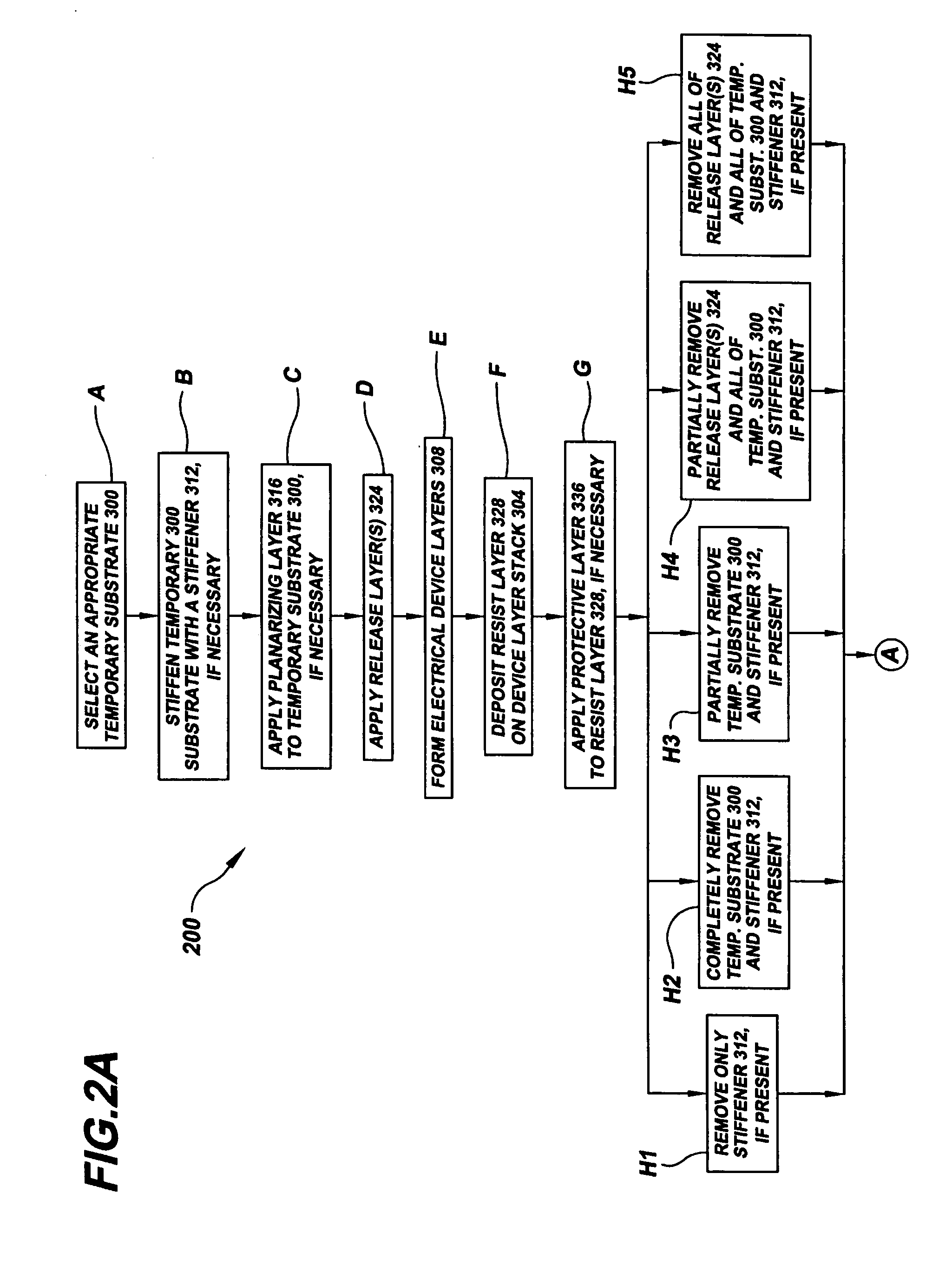
[0160] Referring now to FIGS. 8A-8V, following is an exemplary recipe for making a particular active matrix pixel circuitry sheet 800 (FIG. 8V) of the present invention that may be used as an active matrix backplane of a display device. [0161] Step A: Choose an aluminum metallic foil having a thickness of less than about 20 microns as a temporary substrate 804. [0162] Step B: Attach a stiffener 808 to the backside of temporary substrate 804. For example, stiffener 808 may be a nickel, stainless steel or other metal foil having a thickness of about 100-200 microns. [0163] Step C: Electro-polish the exposed surface of aluminum foil temporary substrate 804 so as to achieve a high degree of planarization of surface 810. [0164] Step D: Deposit a gate metal layer 812. Alternatively, aluminum foil temporary substrate 804 may be alloyed and intrinsically used as a gate metal layer. [0165] Step E: Deposit a silicon nitride (SiNx) layer (coating) 816, an amorphous hydrogenated silicon layer 8...

example 2

[0196] The recipe detailed in Example 1 may be modified for display devices that do not require a transparent TFT backplane. For example, self-emissive devices such as top emitting OLEDs / PLEDs, or reflective devices like electrophoretics, electrochromics, reflective LCDs do not require a backlight for operation. An exemplary modified recipe is as follows. It is noted that steps A-L in the following recipe are identical to Steps A-L revealed in Example 1, above. The following steps are illustrated in corresponding respective FIGS. 9A-9V. [0197] Step A: Choose an aluminum metallic foil having a thickness of less than about 20 microns as a temporary substrate 900. [0198] Step B: Attach a stiffener 904 to the backside of temporary substrate 900. For example, stiffener 904 may be a nickel, stainless steel or other metal foil having a thickness of about 100-200 microns. [0199] Step C: Electro-polish the exposed surface of aluminum foil temporary substrate 900 so as to achieve a high degre...

example 3

[0220] The recipe detailed in Example 2 may be further modified for displays that do not require a transparent TFT backplane. An exemplary modified recipe is as follow. It is noted that Step A-L in the following recipe are identical Steps A-L revealed in each of Examples 1 and 2, above. FIGS. 10A-10U illustrate the following corresponding respective steps. [0221] Step A: Choose an aluminum metallic foil having a thickness of less than about 20 microns as a temporary substrate 1000. [0222] Step B: Attach a stiffener 1004 to the backside of temporary substrate. For example, stiffener may be a nickel, stainless steel or other metal foil having a thickness of about 100-200 microns. [0223] Step C: Electro-polish the exposed surface of aluminum foil temporary substrate 1000 so as to achieve a high degree of planarization on surface 1006. [0224] Step D: Deposit a gate metal layer 1008. Alternatively, aluminum foil temporary substrate 1000 may be alloyed and intrinsically used as a gate met...


PUM


Abstract

A circuitry sheet (322) comprising an electronic device layer stack (304) containing electronic devices, e.g., thin-film transistors, or portions thereof, formed by removing material from both sides of the device layer stack. The circuitry sheet may be made by an electronic/optoelectronic device manufacturing method (200) that includes the steps of forming the device layer stack on a temporary substrate (300), removing material from both sides of the device layer stack, and then attaching a permanent substrate (348) to the device layer stack. The method uses one or more resist layers (600) that may be activated simultaneously and independently to impart distinct circuit pattern images (603, 608, 612) into each of a plurality of image levels (612, 616, 620) within each resist layer, thereby obviating repetitive sequential exposure, registration and alignment steps.

Description

RELATED APPLICATION DATA [0001] This application claims the benefit of priority of U.S. Provisional Patent Application Ser. No. 60 / 608,328, filed Sep. 10, 2004, and titled “Method For Manufacturing Roll To Roll Electronics,” U.S. Provisional Patent Application Ser. No. 60 / 616,530, filed Oct. 7, 2004, and titled “Additional Manufacturing Methods For Roll To Roll Electronics,” and U.S. Provisional Patent Application Ser. No. 60 / 673,519, filed Apr. 22, 2005, titled “Additional Addendum To Method Of Manufacturing Roll To Roll Electronics,” each of which is incorporated by reference herein in its entirety.FIELD OF THE INVENTION [0002] The present invention generally relates to the field of microelectronics and optoelectronics. In particular, the present invention is directed to a microelectronic or optoelectronic circuitry sheet and method of making same. BACKGROUND OF THE INVENTION [0003] The electronic display industry, in its continual quest for increasing efficiency, is constantly sc...

Claims


Application Information

Patent Timeline
IPC IPC(8): H01L21/46
CPCG02F1/133305G02F1/1362G02F1/167G02F2001/13613G02F2001/136231H01L2924/3025H01L21/6835H01L2221/6835H01L2924/19041H01L2924/30105G03F1/144G02F1/1368G02F1/13613G02F1/136231H05K1/16
Inventor JAIN, AJAYKUMAR R.
Owner VERSATILIS
Why Eureka
Try Eureka