Deposition and patterning of boron nitride nanotube ILD

a boron nitride nanotube and patterning technology, applied in the field of semiconductor processing, can solve the problems of most existing dielectric materials, lack of optimal dielectric materials for use in ild, and the need for increased circuit densities and speeds

Inactive Publication Date: 2006-03-23
NXP USA INC
View PDF6 Cites 18 Cited by
  • Summary
  • Abstract
  • Description
  • Claims
  • Application Information

AI Technical Summary

Problems solved by technology

The physical limitations of aluminum interconnects, and in particular their relatively high resistivities, have prevented them from accommodating the need for increased circuit densities and speeds in semiconductor devices.
One of the challenges facing the commercial implementation of dual damascene processes is the lack of an optimal dielectric material for use in the ILD.
In particular, most existing dielectric materials, such as silicon dioxide, porous hydrogen and carbon containing glasses (e.g., SiCOH), or dielectrics based on aromatic hydrocarbon thermosetting polymers, are either unsuitable for use in the ILD layer, are fraught with mechanical stability issues or exhibit k-value integrity issues during processing, or simply have too high of a k-value.
Air gap ILDs possess potentially the best k-value, but come with significant patterning, processing and mechanical integrity challenges.
Other known low-k materials are unsuitable for use in dual damascene processes because they require that a

Method used


Image

  • Deposition and patterning of boron nitride nanotube ILD
  • Deposition and patterning of boron nitride nanotube ILD
  • Deposition and patterning of boron nitride nanotube ILD

Examples


Embodiment Construction

[0020] As used herein, the term “nanoparticle” is meant to encompass nanotubes, nanoballs, nanohorns, and other shapes assumed by materials on the nanoscale.

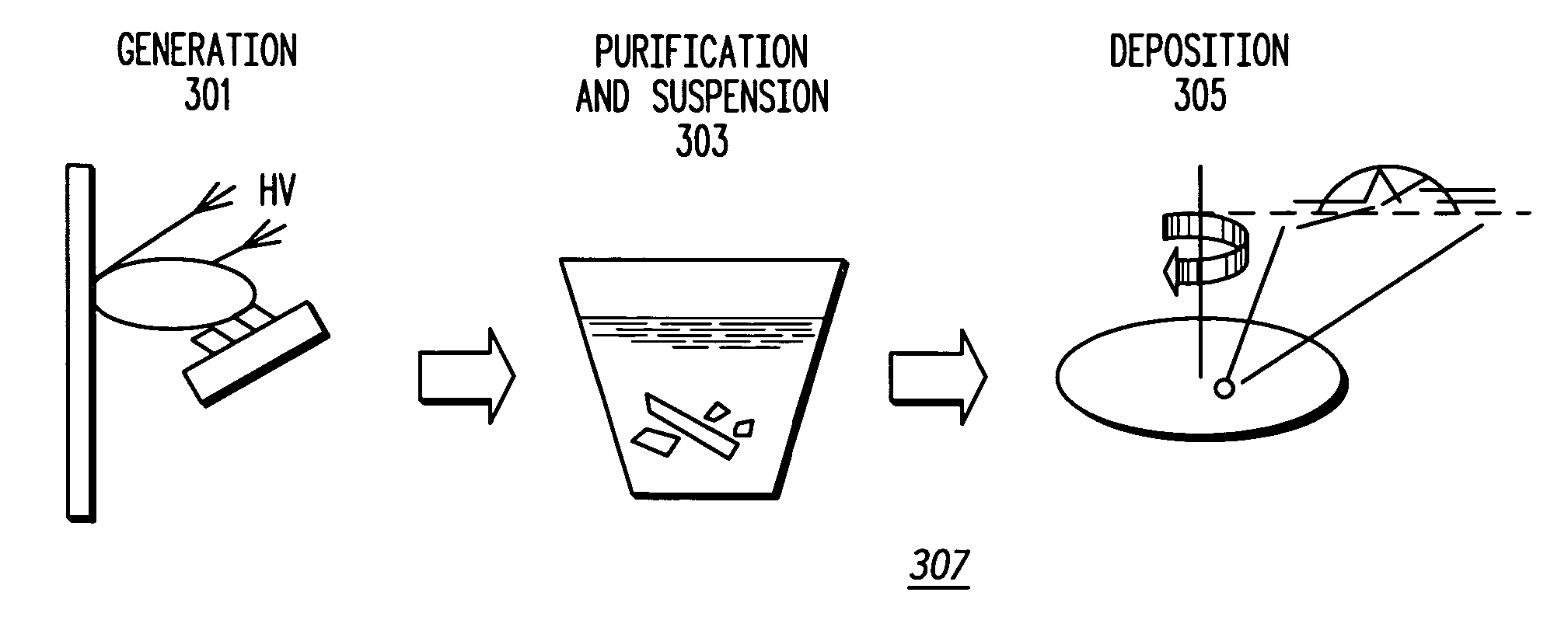
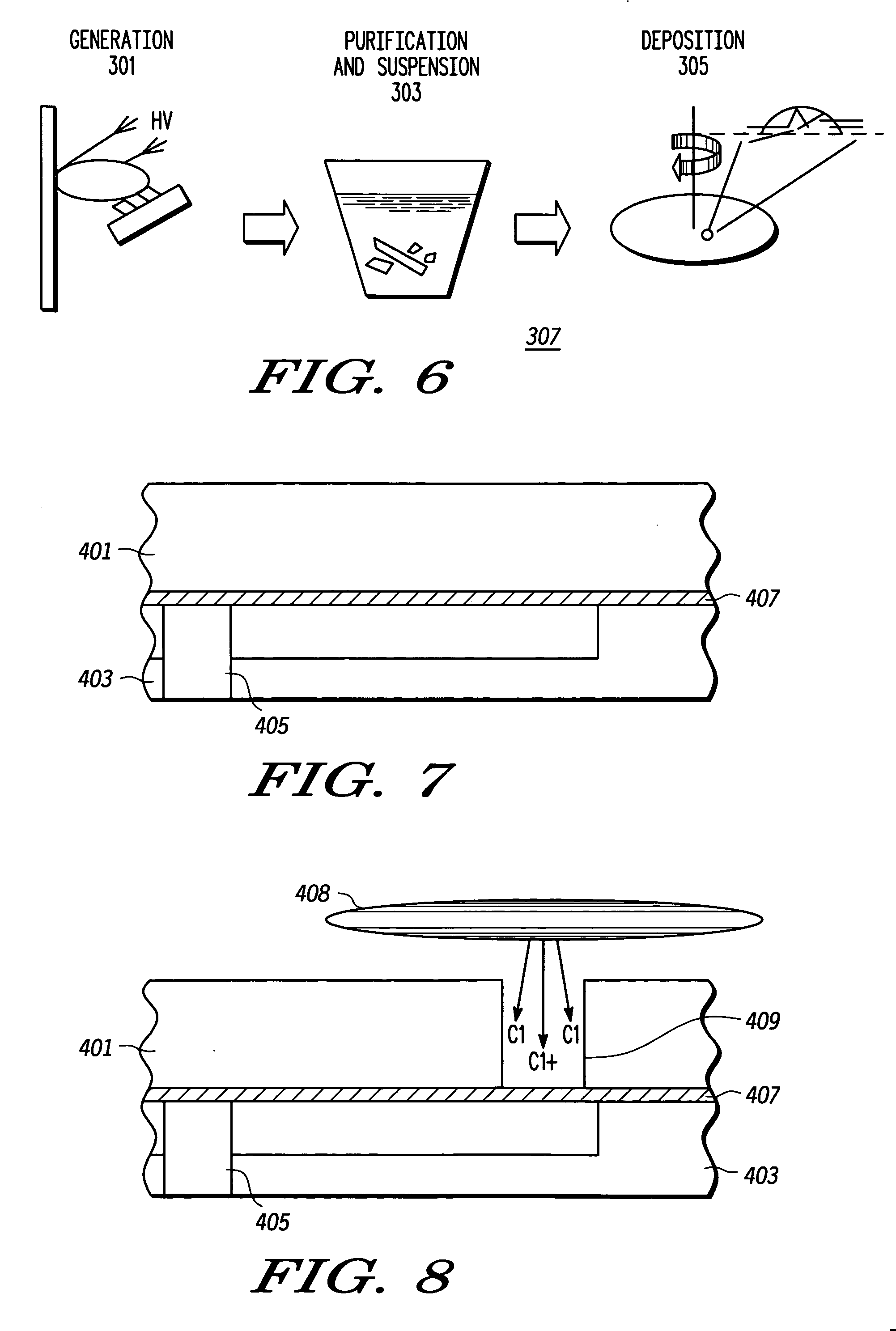
[0021] It has now been found that suspensions of nanoparticles, such as, for example, suspensions of boron-nitride nanotubes (BNNTs) in a liquid medium, can be used to make dielectric layers having low k-values, high structural integrity and excellent mechanical properties. These materials are also conducive to BEOL integration (that is, they are not adversely affected by BEOL etch, metallization and multilayer deposition processes). The use of purified suspensions of BNNTs to make dielectric layers through spin coating or through other evaporative processes is especially preferred, due to the particularly favorable combination of excellent hardness, exceptionally high Young's moduli, and reproducible dielectric constants of 2 or less that these materials and the associated methodology afford.

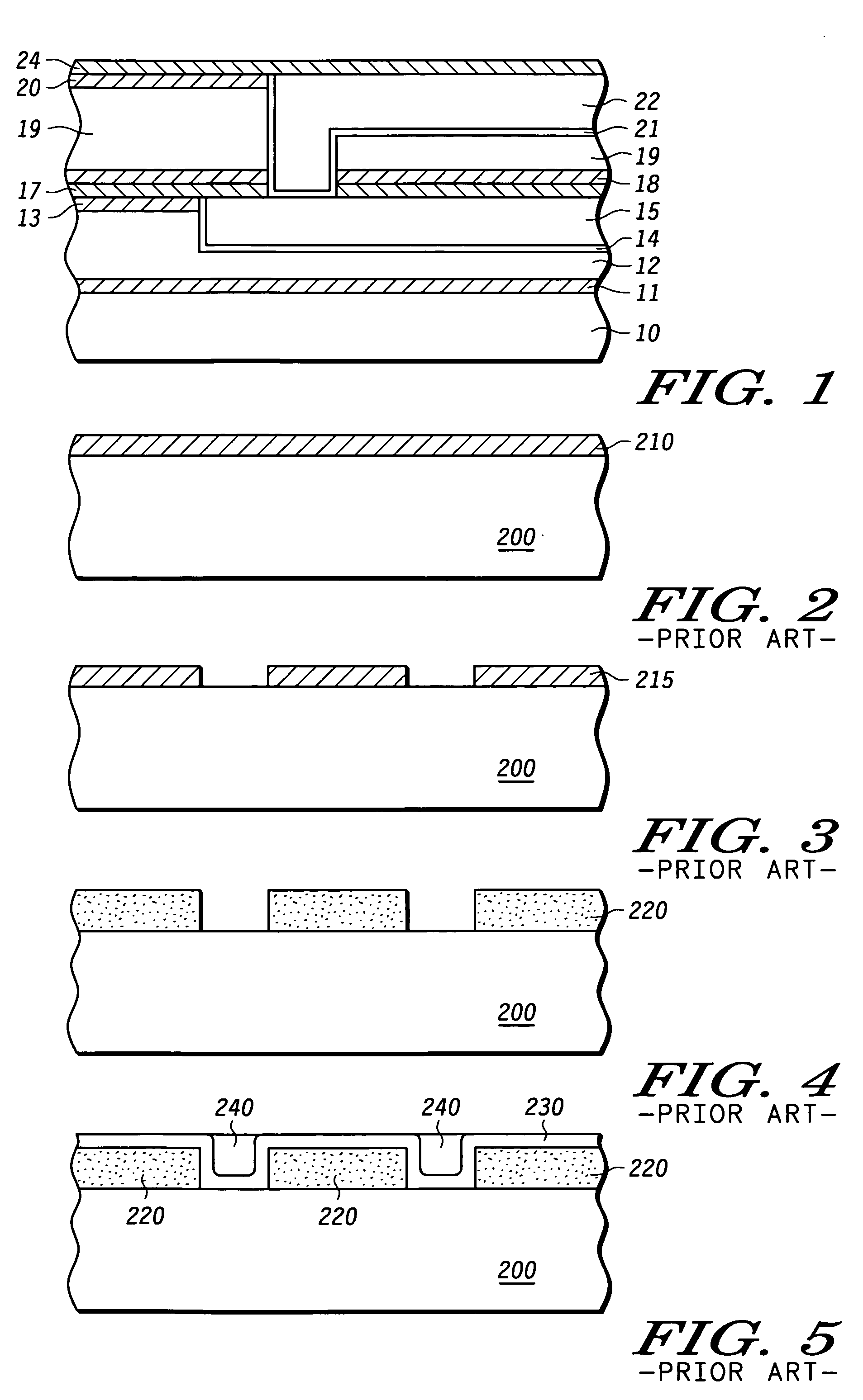
[0022]FIG. 1 illustrates an interc...


PUM


Abstract

A method for forming a dielectric layer is disclosed herein. In accordance with the method, a first material is provided (303) which comprises a suspension of nanoparticles in a liquid medium. A dielectric layer is then formed (305) on the substrate from the suspension through an evaporative process.

Description

FIELD OF THE INVENTION [0001] The present invention relates generally to semiconductor processing, and more particularly to the application of nanoparticle technology in the formation of dielectric layers during semiconductor processing. BACKGROUND OF THE INVENTION [0002] In the past, aluminum and its alloys have been the materials of choice for dual damascene interconnect metallurgies and other Back-End-Of-Line (BEOL) metallization structures utilized in semiconductor devices. These interconnects have typically been embedded in dielectric materials (e.g., SiO2) known as interlayer dielectrics (ILD). The delay in the BEOL structure, and hence its performance characteristics, are dictated by the product of the resistance of the interconnect and the capacitance provided by the ILD materials. [0003] The physical limitations of aluminum interconnects, and in particular their relatively high resistivities, have prevented them from accommodating the need for increased circuit densities an...

Claims


Application Information

Patent Timeline
IPC IPC(8): H01L21/31H01L21/469
CPCB82Y10/00H01L21/318H01L21/76801H01L21/76813H01L2924/0002H01L21/7682H01L23/5329H01L21/76819H01L2924/00H01L21/02282H01L21/02112
Inventor VENTZEK, PETER L.G.JUNKER, KURTORLOWSKI, MARIUS
Owner NXP USA INC
Why Eureka
Try Eureka