CMOS solid-state imaging device and method of manufacturing the same as well as drive method of CMOS solid-state imaging device

a solid-state imaging and imaging device technology, applied in the direction of diodes, semiconductor devices, radiation controlled devices, etc., can solve the problems of difficult three-dimensional cover of the depth direction portion with a sufficient concentration, easy to cause thermal stress defects, and difficult to perform ion implantation

Active Publication Date: 2006-03-30
SONY SEMICON SOLUTIONS CORP
View PDF1 Cites 34 Cited by
  • Summary
  • Abstract
  • Description
  • Claims
  • Application Information

AI Technical Summary

Problems solved by technology

There are mainly two problems with respect to a CMOS solid-state imaging device using the above-described STI element isolation method as a pixel region isolation technology.
However, due to a difference in thermal expansion coefficient between the silicon oxide film 15 deeply buried and the silicon substrates (12 and 13) and other factors, there is a first problem in which pixel defects caused by thermal stress easily occur.
To three-dimensionally cover the portion in the depth direction with a sufficient concentration is not easy from the viewpoint of production thereof.
Specifically, since an impurity is introduced into a narrow place (trench side surface) by portion of diagonal ion implantation, the ion implantation is difficult to be performed.
Further, since the p+ semiconductor region 17 is introduced in an earlier process, there is a problem in which the p+ semiconductor region 17 enlarges a great deal toward the side of a photosensor (photodiode PD) due to thermal diffusion, narrowing the photosensor.
With element isolation by the STI region 81 based on a conventional miniaturization technology, minute isolation can be obtained as an isolation method for a simple MOS transistor; however, with respect to the isolation between pixels of the CMOS solid-state imaging device, there remain the above-described two problems, causing deterioration in images and making it difficult for miniaturized pixels to be manufactured.

Method used


Image

  • CMOS solid-state imaging device and method of manufacturing the same as well as drive method of CMOS solid-state imaging device
  • CMOS solid-state imaging device and method of manufacturing the same as well as drive method of CMOS solid-state imaging device
  • CMOS solid-state imaging device and method of manufacturing the same as well as drive method of CMOS solid-state imaging device

Examples


first embodiment

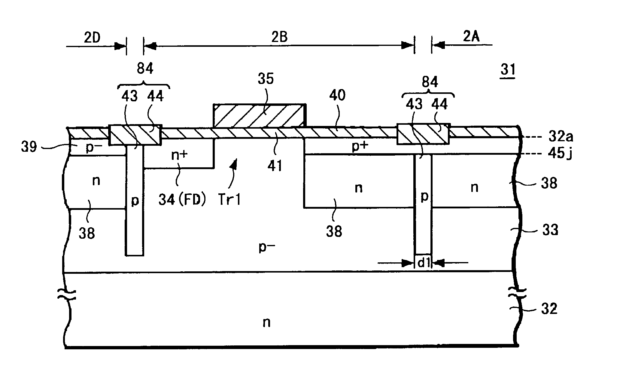
[0038]FIG. 1 shows a CMOS solid-state imaging device according to the present invention. FIG. 1 shows a cross-sectional structure corresponding to the B-B line in the pixel region of FIG. 9.

[0039] In a CMOS solid-state imaging device 31 according to the first embodiment, a second conductive type, for example p-type, semiconductor well region 33 is formed in a first conductive type, for example n-type, silicon semiconductor substrate 32; a plurality of unit pixels 2 [2A, 2B, 2C and 2D], each of which includes a photodiode PD that is a photoelectric conversion portion and a plurality of MOS transistors, are formed in the p-type semiconductor well region 33; and an element isolation region 82, which is element isolation portion according to the present invention, (corresponding to the element isolation region 8 in FIG. 9) is formed between unit pixels 2 next to each other, and also within each unit pixel. In FIG. 1, in the p-type semiconductor well region 33 are formed: a photodiode PD...

second embodiment

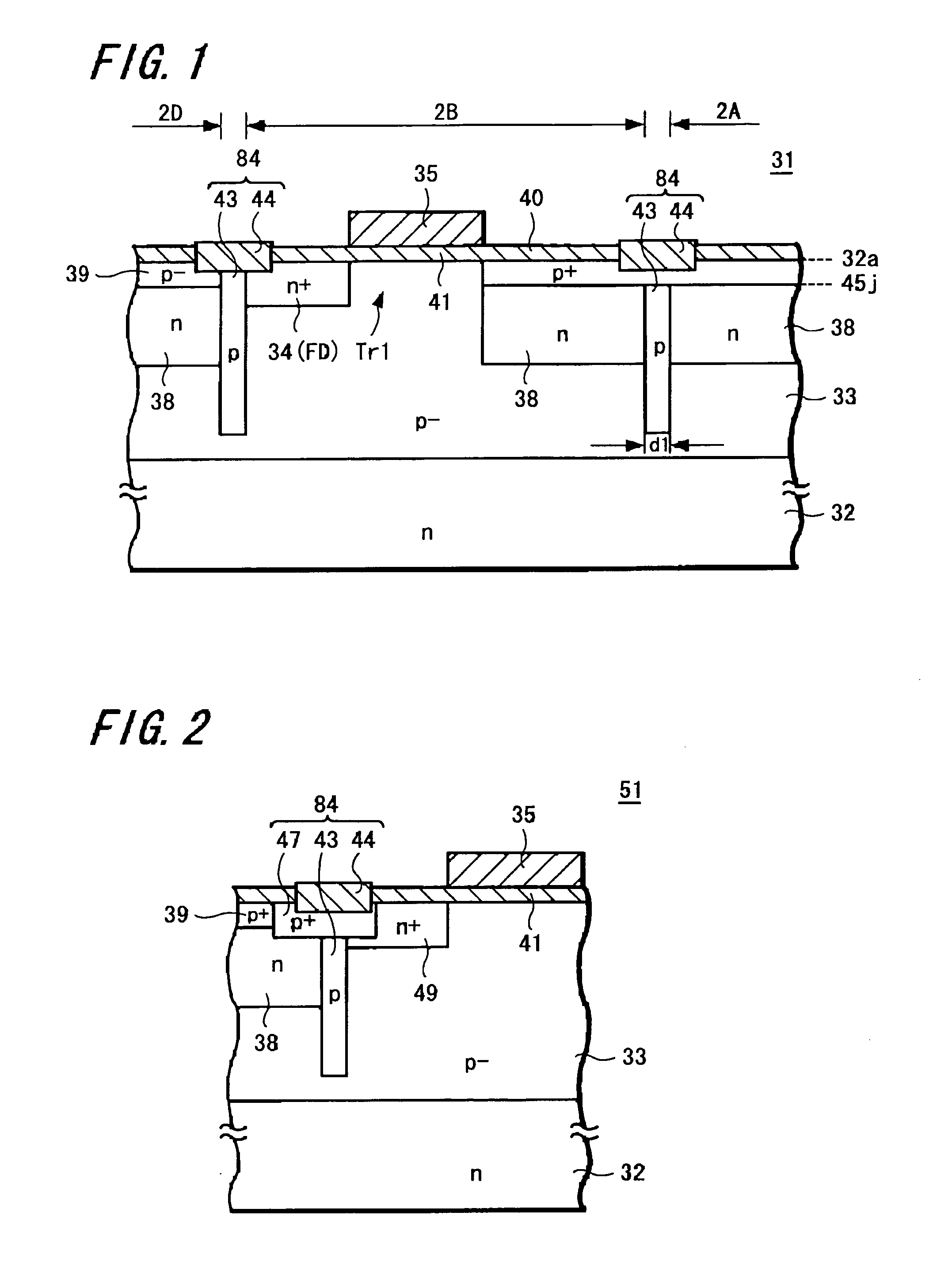
[0051] Next, FIG. 2 shows a CMOS solid-state imaging device according to the present invention. FIG. 2 shows the cross-sectional structure of the relevant part of a pixel region similar to the above described embodiment, and portions corresponding to those in FIG. 1 are given the same numerals and redundant explanations are omitted.

[0052] In a CMOS solid-state imaging device 51 according to the second embodiment, an element isolation region 83 (corresponding to the element isolation region 8 in FIG. 9) which isolates a floating diffusion (FD) and the other MOS transistor source drain region 49 from a photodiode PD of an adjacent pixel is formed of a first p-type isolation diffusion layer 43, a second p-type isolation diffusion layer 47 thereon, and an isolation oxide film 44 further thereon. The second isolation diffusion layer 47 is made to have impurity concentration equal to or higher than that of a p+ accumulation layer 39. With respect to other structures than that, detailed ex...

third embodiment

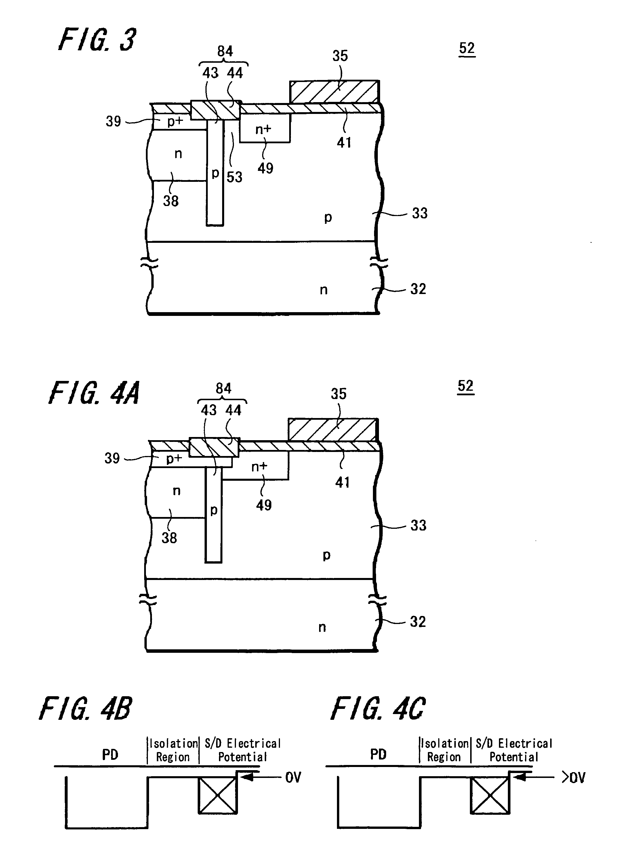
[0055]FIG. 3 shows a CMOS solid-state imaging device according to the present invention. FIG. 3 shows the cross-sectional structure of the relevant part of a pixel region similar to the above described embodiment, and portions corresponding to those in FIG. 1 are given the same numerals and redundant explanations are omitted.

[0056] In a CMOS solid-state imaging device 52 according to the third embodiment, an element isolation region 84 (corresponding to the element isolation region 8 in FIG. 8) formed of a p-type isolation diffusion layer 43 and an isolation oxide film 44 thereon is formed between a floating diffusion (FD) and the other MOS transistor source drain region 49 and a photodiode PD of an adjacent pixel.

[0057] In this embodiment, particularly in the case that the impurity concentration of the floating diffusion (FD) and the other MOS transistor source drain region 49 and the p-type isolation diffusion layer 43 of the element isolation region is high, a separation region ...


PUM


Abstract

In a CMOS solid-state imaging device, to restrain the occurrence of white spots and dark current caused by pixel defects, and also to increase the saturation signal amount.
Adjacent pixels 2A and 2B are separated by element isolation portion 82 formed of a diffusion layer 43 and an insulating layer 44 thereon, and the insulating layer 44 of the element isolation portion 82 is formed in a position equal to or shallower than the position 45j of a pn junction on the side of accumulation layer 39 of a photoelectric conversion portion constituting a pixel.

Description

CROSS PREFERENCE TO RELATED APPLICATIONS [0001] The present invention claims the benefit of Japanese Patent Application JP P2004-275461 filed in the Japanese Patent Office on Sep. 22, 2004, the entire contents of which are incorporated herein by reference. FIELD OF THE INVENTION [0002] The present invention relates to a CMOS solid-state imaging device, a method of manufacturing the same, and a drive method of the CMOS solid-state imaging device. BACKGROUND OF THE INVENTION [0003] Generally, in the MOS type semiconductor device, LOCOS (local oxidization of silicon) isolation has been used as element isolation for a long time, and STI (shallow trench isolation) has been come to use in recent years due to the miniaturization thereof. [0004] In the CMOS solid-state imaging device as well, the STI has been used for element isolation. A CMOS solid-state imaging device includes a pixel region and peripheral circuitry which drives the pixel and performs signal processing, and a miniaturizat...

Claims


Application Information

Patent Timeline
Patent Type & Authority Applications(United States)
IPC IPC(8): H01L29/76
CPCH01L27/1463H01L27/14689H01L27/14687H01L27/14643H01L27/14
Inventor ABE, HIDESHITATANI, KEIJIITONAGA, KAZUICHIRO
Owner SONY SEMICON SOLUTIONS CORP
Why Eureka
Try Eureka