Semiconductor device with double barrier film
a technology of barrier film and semiconductor, applied in the direction of semiconductor device, semiconductor/solid-state device details, electrical apparatus, etc., can solve the problems of deteriorating device reliability, disadvantageous fine patterning, and difficult to microfabricate contacts by so-called lithography technology
- Summary
- Abstract
- Description
- Claims
- Application Information
AI Technical Summary
Benefits of technology
Problems solved by technology
Method used
Image
Examples
first embodiment
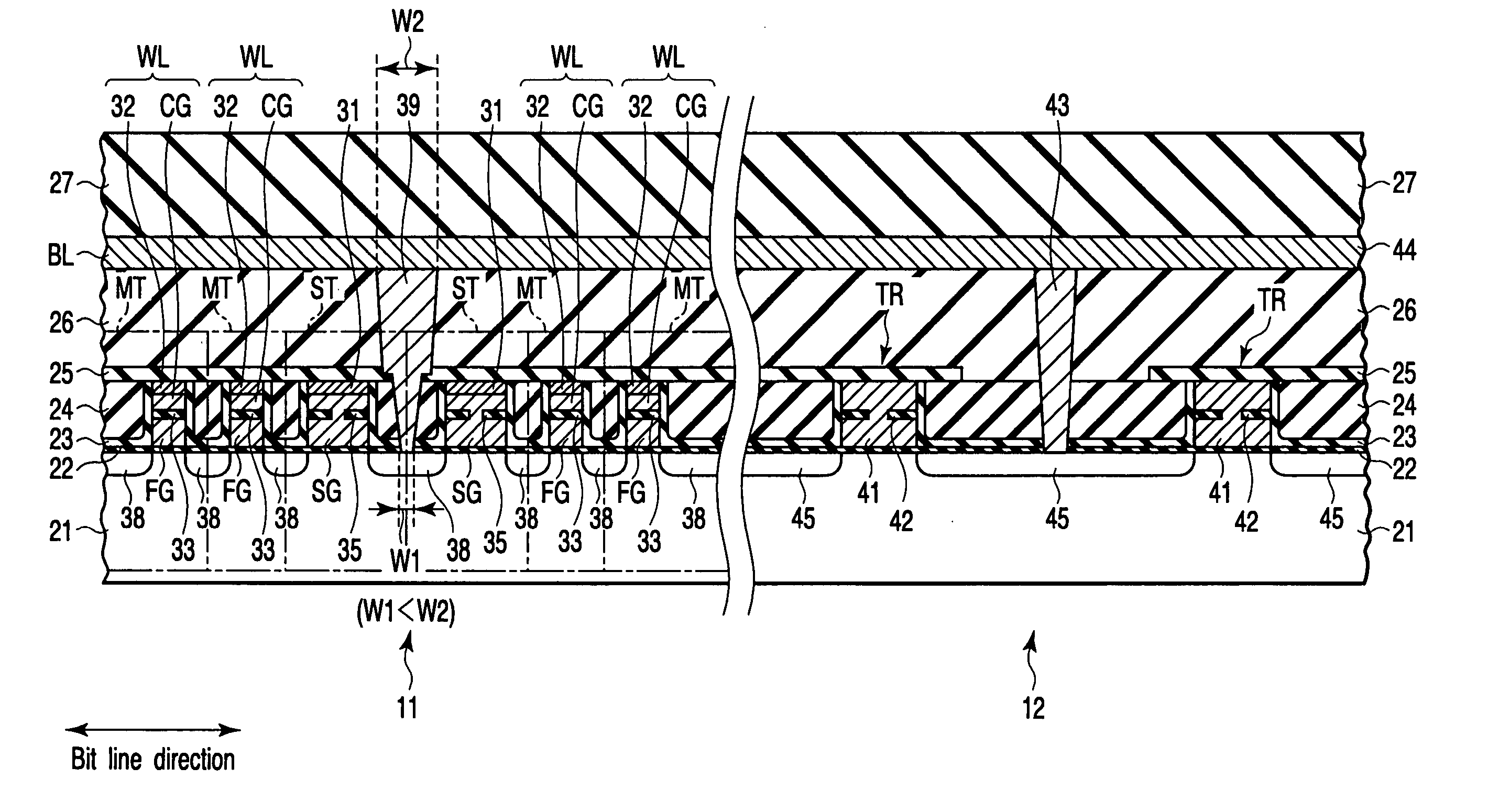
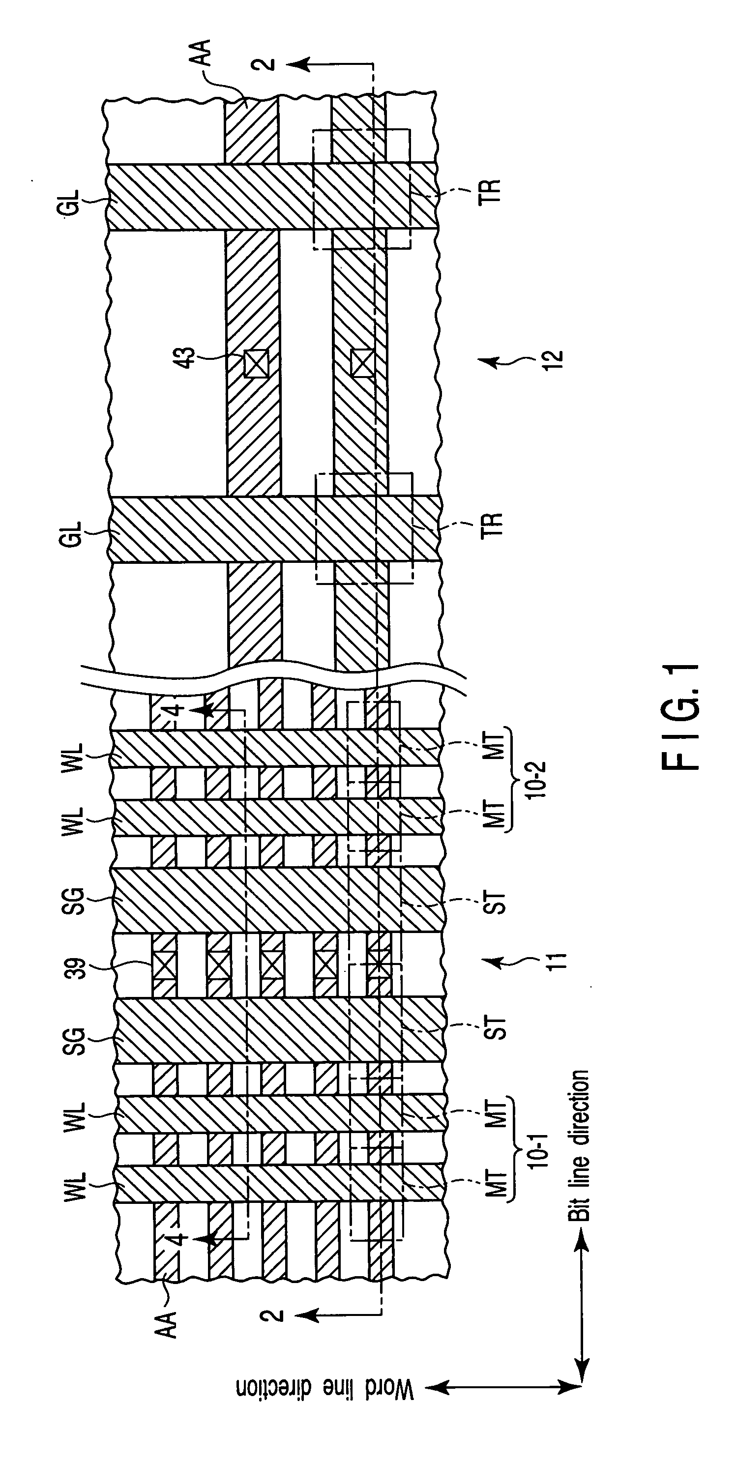
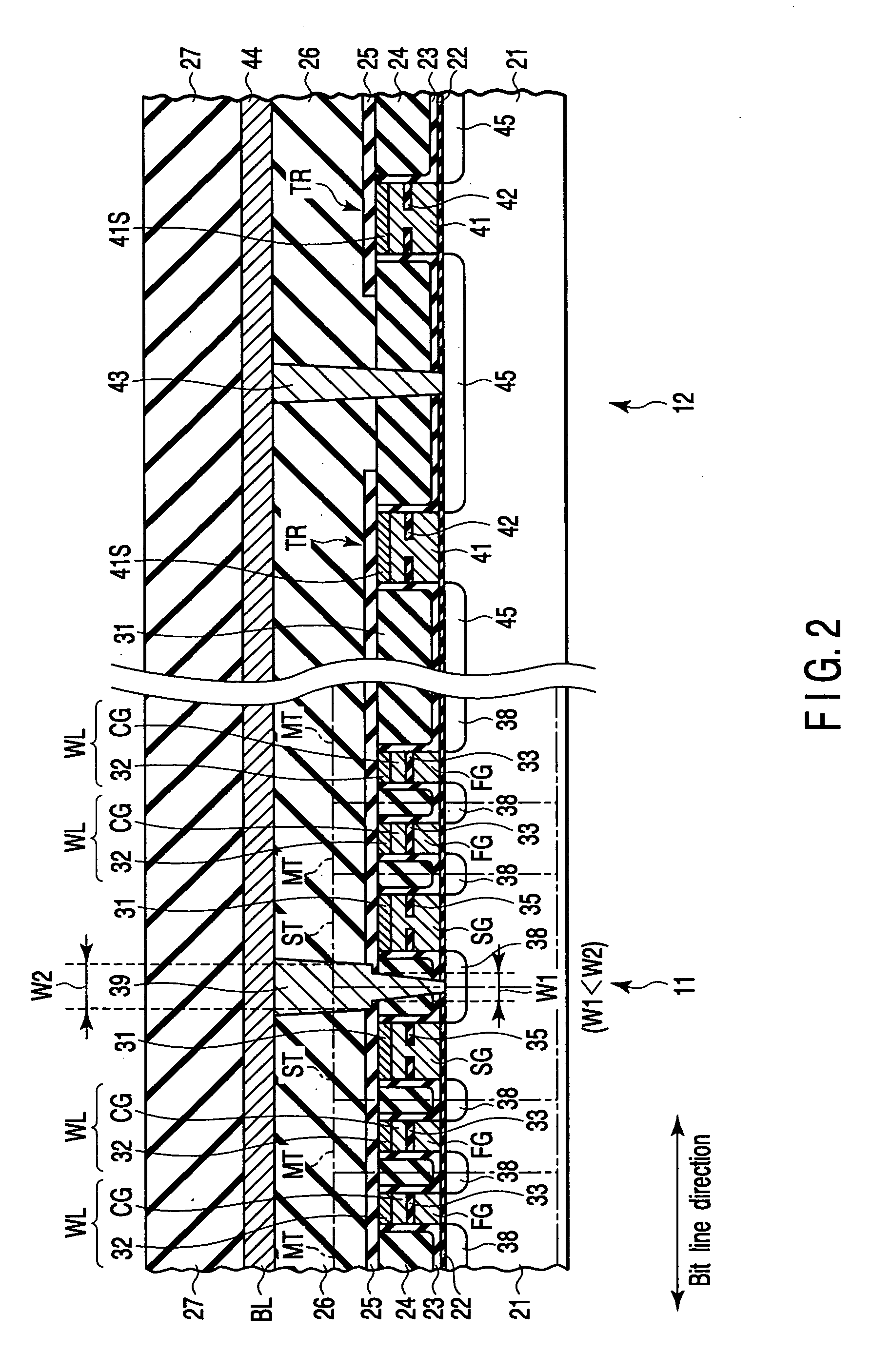
[0048] The structure of a semiconductor device according to a first embodiment of the invention is described referring to FIG. 1 to FIG. 4.
[0049]FIG. 1 is a plan view that schematically shows the semiconductor device according to the first embodiment. FIG. 2 is a cross-sectional structural view taken along line 2-2 in FIG. 1. FIG. 3 is a cross-sectional structural view that shows, in enlarged scale, a contact plug 39 near a barrier film 25 in FIG. 2. FIG. 4 is a cross-sectional structural view taken along line 4-4 in FIG. 1. In this embodiment, a NAND type flash memory is described by way of example.
[0050] As is shown in the Figures, a memory cell array 11 and a peripheral circuit 12 are provided on a major surface of a semiconductor (silicon) substrate 21.
[0051] The memory cell array 11 includes memory cell rows 10-1 and 10-2 that are arranged in a bit line direction, and select transistors ST. The select transistors ST select memory cell rows 10-1 and 10-2.
[0052] The memory ce...
modification 1 (
[Modification 1 (Modification of Etching Mask)]
[0107] A method of manufacturing a semiconductor device according to Modification 1 of the present invention will now be described with reference to FIG. 15 and FIG. 16. Modification 1 relates to the photoresist 60 in the above-described first embodiment. FIG. 15 and FIG. 16 are plan views that schematically show a photoresist 60 for use in the manufacturing method of the semiconductor device according to Modification 1. A description of the parts common to those of the first embodiment is omitted.
[0108] A photoresist 60 shown in FIG. 15 has a trench 61 that is formed in the word line direction with a width W2 greater than the width W1. With this photoresist 60, a so-called common source line is formed, wherein the diffusion layers 38 of the select transistors ST arranged along the word line direction cab be set at an equal potential.
[0109] A photomask 60 shown in FIG. 16 has circular opening portions 61 each having a diameter W2 that...
modification 2 (
[Modification 2 (Modification of Peripheral Circuit)]
[0114] A method of manufacturing a semiconductor device according to Modification 2 of the present invention will now be described with reference to FIG. 17 through FIG. 19. FIG. 17 is a cross-sectional view that schematically shows the structure of a semiconductor device according to Modification 2. FIG. 18 and FIG. 19 are cross-sectional structural views that schematically illustrate fabrication steps of the semiconductor device according to Modification 2. Modification 2 relates to the gate line GL of the peripheral circuit 12 in the first embodiment. A description of the parts common to those in the first embodiment is omitted.
[0115] According to the semiconductor device of Modification 2, the same advantageous effects as with the first embodiment are obtained. In addition, as shown in the Figures, the gate line GL of the peripheral transistor TR of the peripheral circuit 12 is not provided with a silicide layer. Thus, the se...
PUM
 Abstract
Description
Claims
Application Information


