Nonvolatile memory structure

a non-volatile, memory technology, applied in static storage, digital storage, instruments, etc., can solve the problems of increasing process integration difficulty and cost overhead, large cell size in the conventional design, and not suitable for embedded flash/eeprom applications

Active Publication Date: 2006-03-30
SOLID STATE SYST
View PDF8 Cites 58 Cited by
  • Summary
  • Abstract
  • Description
  • Claims
  • Application Information

AI Technical Summary

Benefits of technology

[0010] The invention provides a novel design of a nonvolatile memory device, which can at least solve the conventional drawbacks.

Problems solved by technology

However, incompatibility process between conventional stack gate EPROM / FLASH memory and CMOS LOGIC process leads to increase process integration difficulty and cost overhead.
However the space-apart region of N-well capacitor and EPROM cell causes a large cell size in the conventional design.
This is because of device isolation limitation between P+ Diffusion in N-well to N+ Diffusion in P-well.
Also and, it is not suitable for embedded Flash / EEPROM applications because the over-erase issue may be caused.

Method used


Image

  • Nonvolatile memory structure
  • Nonvolatile memory structure
  • Nonvolatile memory structure

Examples


Embodiment Construction

[0031] In general, the invention at least introduce, for example, a single poly electrically programmable EPROM cell by utilizing an N-well inversion capacitor as control gate to couple program / read operation voltage to floating gate. One selected gate in series with floating gate are formed by the same poly-silicon layer to prevent over-erase issue. A new program operation condition is also proposed to prevent program disturbing issue by inserting program preset cycle. Regarding to process, the present invention of EPROM cell can be manufactured with standard CMOS Logic Process.

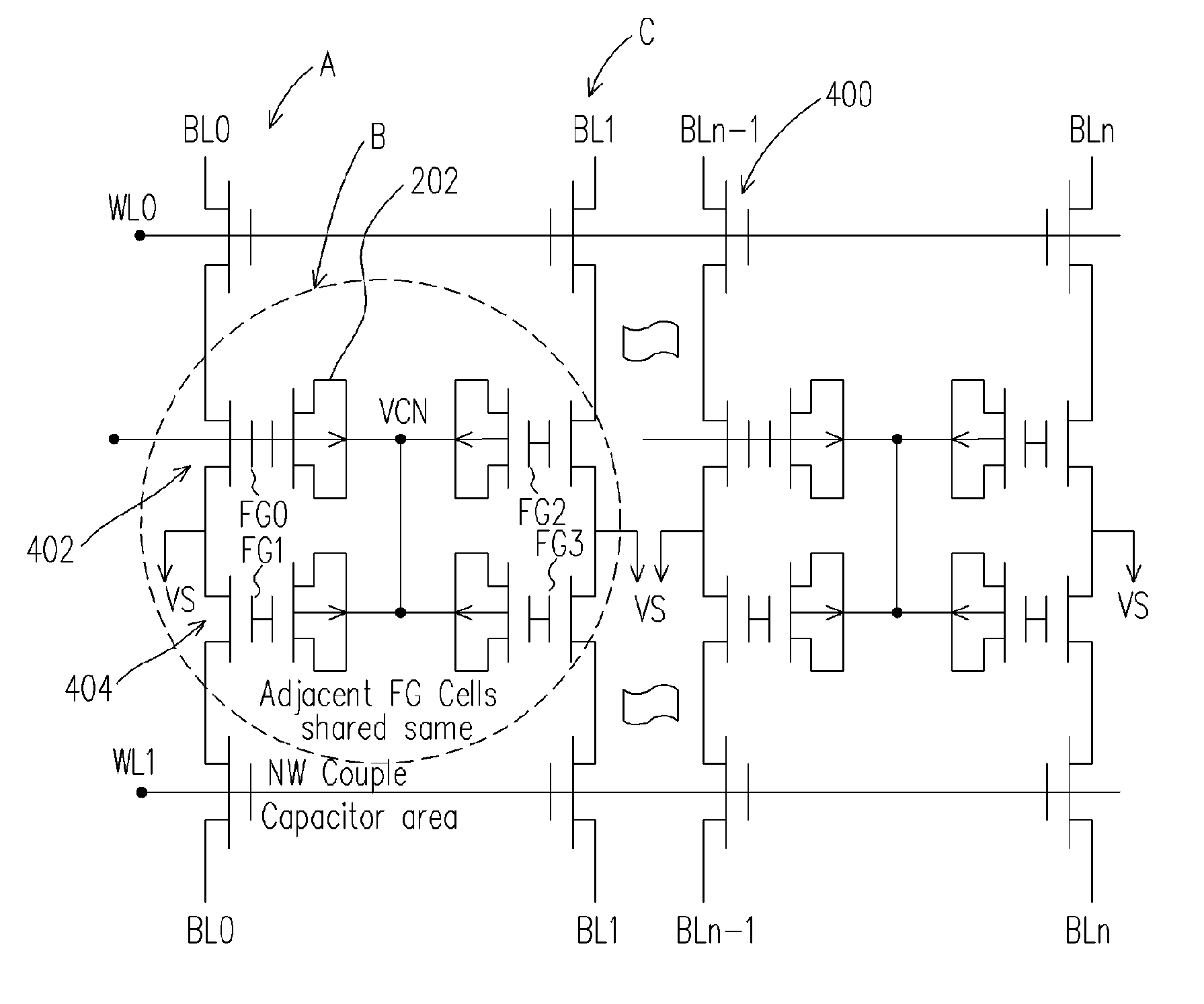
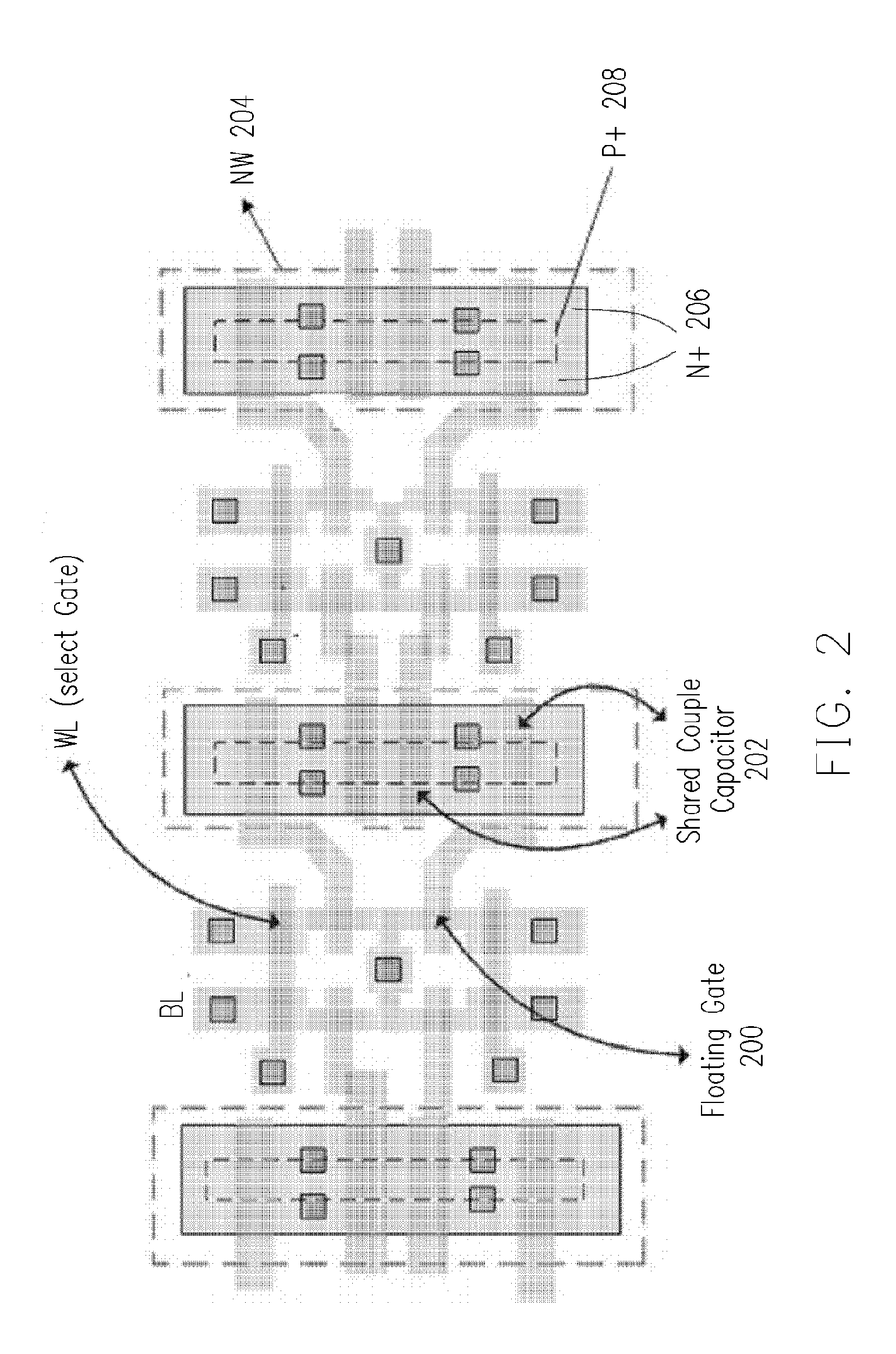
[0032] In order to reduce the cell size, a novel design of compact single-poly EPROM / EEPROM memory cell that is named as Shared Couple Capacitor Single Poly EPROM / EEPROM (SCCSP Cell as shown in FIG. 2) is proposed. In FIG. 2, two adjacent EPROM / EEPROM cells utilize the same shared couple capacitor 202 that is made of N-well capacitor with P+ / N+ diffusion butting contact. P+ Diffusion in the middle of the sh...


PUM


Abstract

The invention is directed to a layout of nonvolatile memory device. The memory cell has a gate electrode, a first doped electrode, and a second doped electrode. The first doped electrode is coupled to the bit line. The gate electrode is coupled to one separated word line. A shared coupled capacitor structure is coupled between all of memory cells of the adjacent bit lines from the second doped electrode. The capacitor structure has at least two floating-gate MOS capacitors. Each floating-gate MOS capacitor has a floating-gate transistor having a floating gate, a first S / D region and a second S / D region; and a MOS capacitor coupled to the floating gate. The first S / D region is coupled to the second doped electrode of the corresponding one of the transistor memory cells, and the second S / D region is shared with an adjacent one of the floating-gate transistor.

Description

CROSS-REFERENCE TO RELATED APPLICATION [0001] This application is a divisional of a prior application Ser. No. 10 / 707,665, filed Dec. 31, 2003.BACKGROUND OF THE INVENTION [0002] 1. Field of Invention [0003] The present invention relates to Non-volatile memory structure. More particularly, the present invention relates to a non-volatile memory device with CMOS logic process. [0004] 2. Description of Related Art [0005] Non-volatile memory has its wide applications in various field, such as the multimedia or particularly to the portable multi-media applications including digital camera and audio player, or the smart cellular phone. All of these apparatus need to store data or contents when power is off. Nonvolatile memory then has various applications. [0006] In the various applications for integration nonvolatile memory, from fabrication and operation point of view, it is desired to adapted in the standard CMOS LOGIC process. Those applications include software updates, storing ID cod...

Claims


Application Information

Patent Timeline
Patent Type & Authority Applications(United States)
IPC IPC(8): G11C16/04G11C16/34
CPCG11C16/3468
Inventor LEE, CHIEN-HSINGLIN, CHIN-HSILIOU, JHYY-CHENG
Owner SOLID STATE SYST
Why Eureka
Try Eureka