Easily crack checkable semiconductor device

Inactive Publication Date: 2006-04-06
DENSO CORP
View PDF4 Cites 11 Cited by
  • Summary
  • Abstract
  • Description
  • Claims
  • Application Information

AI Technical Summary

Benefits of technology

[0010] The crack inspection can be conducted without disassembling the package or disconnecting the wiring, i.e., without destruction of the device.

Problems solved by technology

The crack typically occurs in an interlayer insulation film of the semiconductor device during a wire bonding process, a packaging process, or an endurance test.
It takes much time and effort to detect the crack using the visual inspection me

Method used


Image

  • Easily crack checkable semiconductor device
  • Easily crack checkable semiconductor device
  • Easily crack checkable semiconductor device

Examples


first embodiment

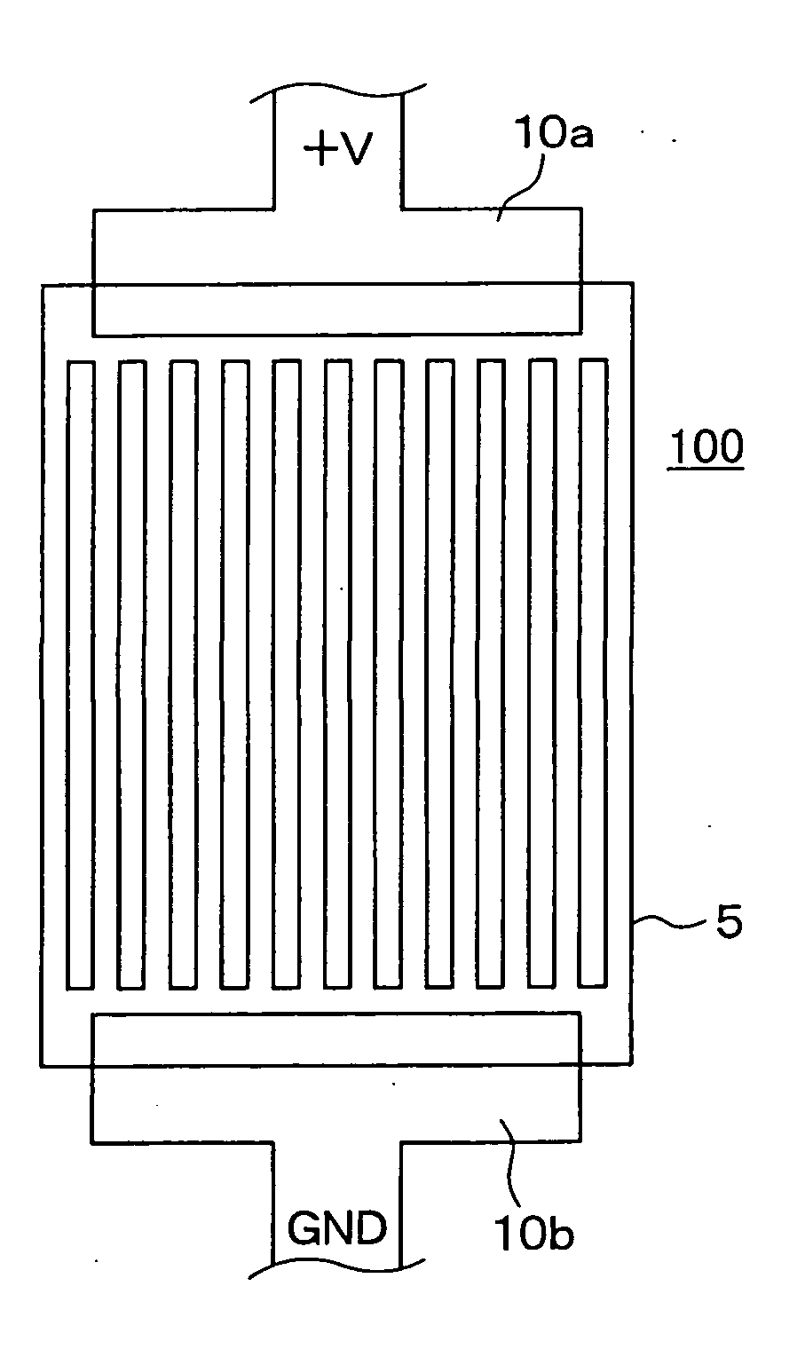
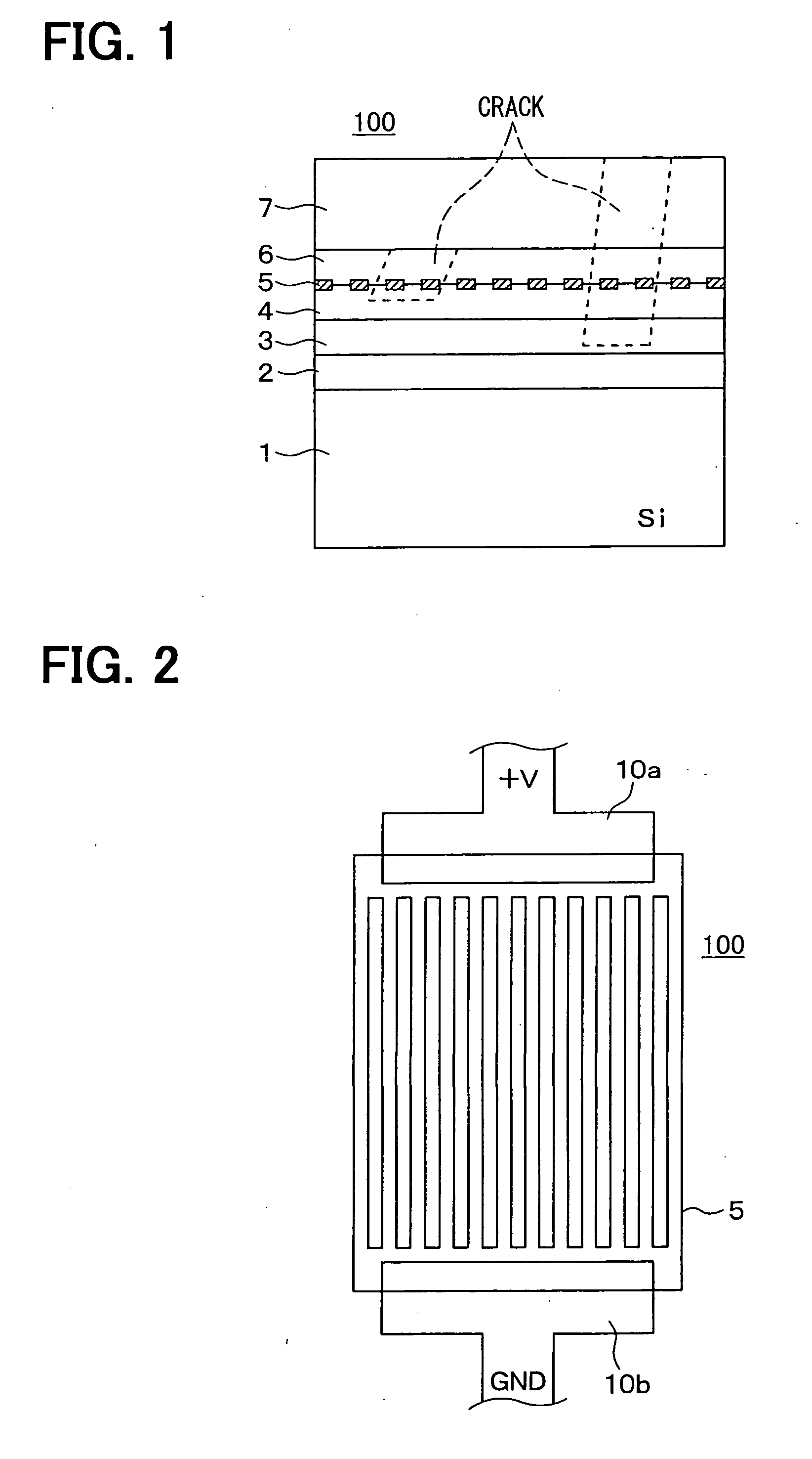
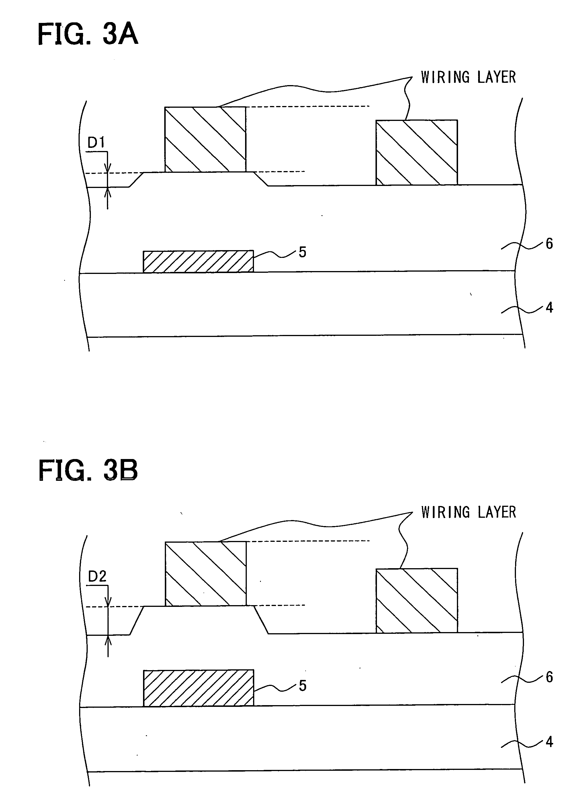
[0019] A semiconductor device 100 according to a first embodiment of the present invention is shown in FIGS. 1 and 2. The device 100 includes a silicon substrate 1, a field oxide film 2 disposed on the substrate 1, a boron-doped phosphor-silicate glass (BPSG) film 3 disposed on the field oxide film 2, a first tetraethylorthosilicate (TEOS) film 4 disposed on the BPSG film 3, a thin film resistor 5 disposed on the first TEOS 4, a second TEOS film 6 disposed on the thin film resistor 5, and a protective film 7 disposed on the second TEOS film 6.

[0020] Specifically, the thin film resistor 5 is disposed on a surface of the first TEOS film 4 as a first insulation film, after the field oxide film 2, the BPSG film 3, and the first TEOS film 4 are stacked in this order on the substrate 1. Then, the second TEOS film 6 as a second insulation film covers the thin film resistor 5, and the protective film 7 covers a surface of the second TEOS film 6.

[0021] Disposing the thin film resistor 5 on...

second embodiment

[0051] A semiconductor device 200 according to a second embodiment of the present invention is shown in FIGS. 6 and 7. The device 200 includes a Laterally Diffused Metal Oxide Semiconductor (LDMOS) element.

[0052] The LDMOS element is formed on a substrate 13. The substrate 13 is constructed by forming an N−-type layer 12 on an N+-type silicon substrate 11. A LOCOS (local oxidation of silicon) oxide film 14 is formed on the surface of the N−-type layer 12. An N+-type drain region 15 of high impurity concentration is formed in the surface of the N−-type layer 12 to contact with the LOCOS oxide film 14. An N-type well 16 is formed to surround the N+-type drain region 15 and extends under the LOCOS oxide film 14. In the N-type well 16, impurity concentration decreases with distance from the N+-type drain region 15.

[0053] A P-type base region 17 is formed on the surface of the N−-type layer 12. The P-type base region 17 is terminated near the edge of the LOCOS oxide film 14. An N+-type...


PUM


Abstract

A semiconductor device includes a first insulation film, a second insulation film, a thin film resistor interposed between the insulation films. A predetermined voltage is applied to the thin film resistor so that a current flows through the thin film resistor. When a crack occurs in the insulation films, the thin film resistor is partially destroyed and the resistance of the thin film resistor changes. The crack is detected by measuring the change in resistance of the thin film resistor based on the predetermined voltage and the current flowing through the thin film resistor. Therefore, a crack inspection can be conducted without destruction of the device.

Description

CROSS REFERENCE TO RELATED APPLICATION [0001] This application is based on Japanese Patent Application No. 2004-290119 filed on Oct. 1, 2004, the disclosure of which is incorporated herein by reference. FIELD OF THE INVENTION [0002] The present invention relates to a semiconductor device, to which a crack inspection can easily apply. BACKGROUND OF THE INVENTION [0003] In a manufacturing process of a semiconductor device, an inspection for detection of a crack is conducted. The crack typically occurs in an interlayer insulation film of the semiconductor device during a wire bonding process, a packaging process, or an endurance test. In the method used for the crack detection, the chip surface of the device is visually inspected, because a semiconductor element is disposed on the chip surface. Therefore, the chip surface is required to be exposed by disassembling the package or disconnecting the wiring. [0004] It takes much time and effort to detect the crack using the visual inspecti...

Claims


Application Information

Patent Timeline
IPC IPC(8): H01L29/76
CPCH01L21/31612H01L21/31625H01L22/34H01L2924/0002H01L2924/00H01L21/02129
Inventor TAI, AKIRANAKAYAMA, YOSHIAKI
Owner DENSO CORP
Why Eureka
Try Eureka