Interference optical switch and variable optical attenuator

Active Publication Date: 2006-04-06
NIPPON TELEGRAPH & TELEPHONE CORP
View PDF3 Cites 27 Cited by
  • Summary
  • Abstract
  • Description
  • Claims
  • Application Information

AI Technical Summary

Benefits of technology

[0036] The present invention is implemented to solve the foregoing problems of the above-described conventional techniques. Therefore it is an object of the present invention to p

Problems solved by technology

In practice, however, it is difficult to maintain the power coupling ratios of the WINCs at 0.5 over a broad wavelength band because of the fabrication error and the like.
Thus, the wavelength characteristics are deteriorated by deviation of the power coupling ratios.
The conventional interferometer optical switches or variable optical attenuators, however, have the following problems.
However, if the power coupling ratio of the directional couplers becomes r1=r2=0.4 because of the fabrication error, for example, the conditions for the high extinction ratio are not satisfied, thereby deteriorating the extinction ratio markedly.
Thus, because of the fabrication error and wavelength dependence of the optical couplers, the conventional symmetric Mach-Zehnder interferometer optical switch cannot be used in a broad band.
Hence, it is not suitable for wavelength division multiplexing tr

Method used


Image

  • Interference optical switch and variable optical attenuator
  • Interference optical switch and variable optical attenuator
  • Interference optical switch and variable optical attenuator

Examples


first embodiment

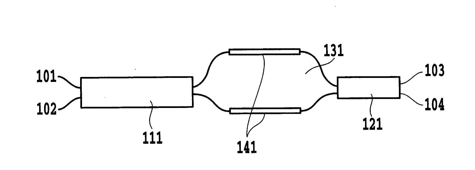
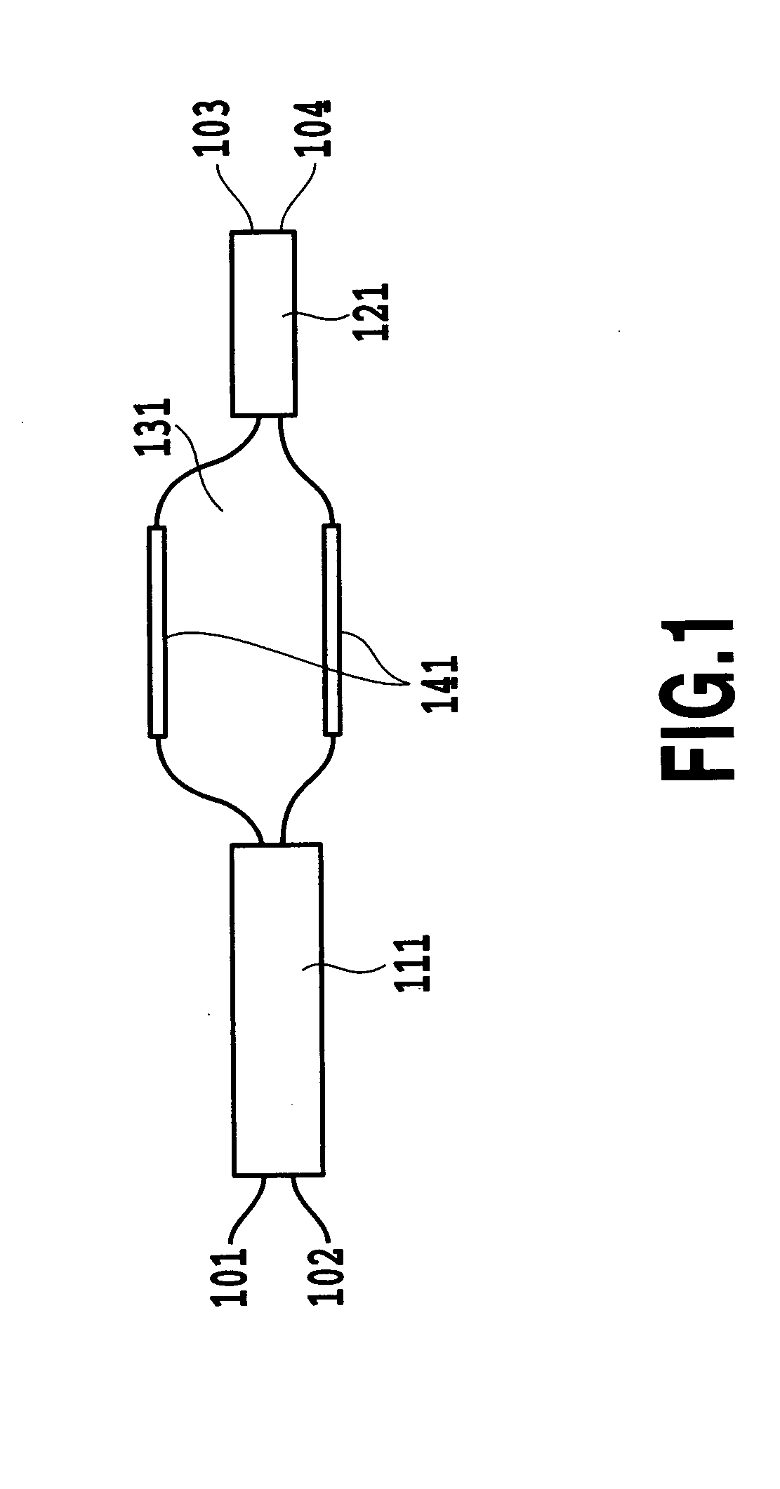
[0116]FIG. 1 shows a configuration of the interferometer optical switch of a first embodiment in accordance with the present invention.

[0117] The interferometer optical switch of the present embodiment includes an optical multi / demultiplexing device (phase generating coupler) 111, the phase difference of the output of which has wavelength dependence; an optical multi / demultiplexing device 121; an optical delay line 131 between the optical multi / demultiplexing devices 111 and 121; phase shifters 141 formed in the optical delay line 131; input waveguides 101 and 102; and output waveguides 103 and 104.

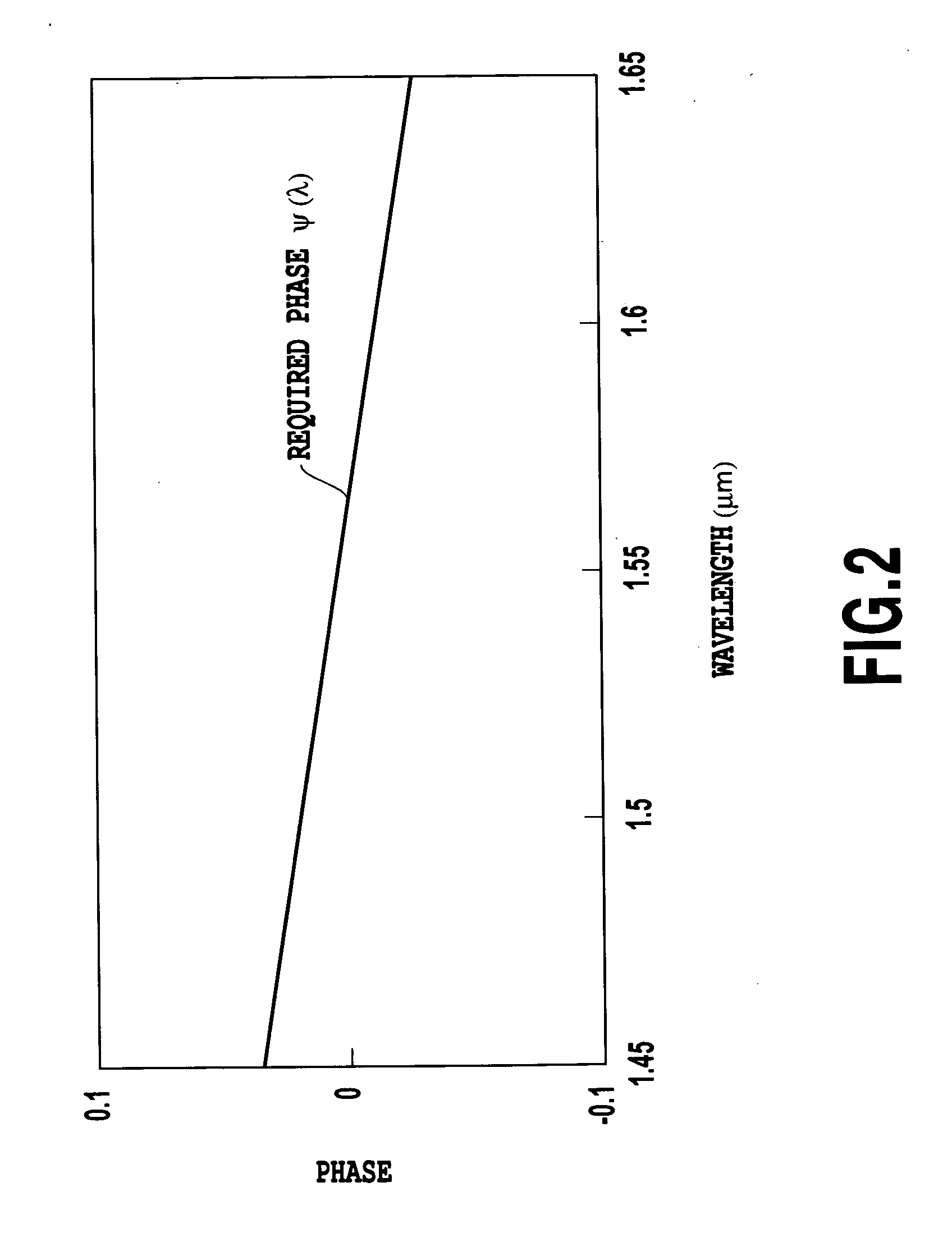
[0118] The transmission characteristics of the Mach-Zehnder interferometer is illustrated in FIG. 41A. it has a high extinction ratio at the signal wavelength λs, but the extinction ratio deteriorates as the wavelength departs from the signal wavelength. It will be possible to maintain a high extinction ratio throughout the wavelength region if the entire wavelength region can be made t...

second embodiment

[0155]FIG. 11 shows a configuration of the interferometer optical switch of a second embodiment in accordance with the present invention. The circuit of the interferometer optical switch includes a pair of optical multi / demultiplexing devices (phase generating couplers) 111 and 112, the phase differences of the outputs of which have wavelength dependence; an optical delay line 131 between the optical multi / demultiplexing devices 111 and 112; phase shifters (thin film heaters) 141 formed in the optical delay line 131; input waveguides 101 and 102; and output waveguides 103 and 104.

[0156] In the present embodiment, a configuration will be described which includes a plurality of phase generating couplers. Assume that a light is input to the phase generating coupler 111 in the first stage, and the phase difference between light output from the two optical waveguides connected to the phase generating coupler 111 is φ1(λ); and that light are launched into the two optical waveguides conne...

third embodiment

[0168]FIG. 15 shows a configuration of the interferometer optical switch of a third embodiment in accordance with the present invention. The circuit of the interferometer optical switch of the present embodiment includes an optical multi / demultiplexing device (phase generating coupler) 111, the phase difference of the output of which has wavelength dependence; a directional coupler 153; an optical delay line 131 between the optical multi / demultiplexing device 111 and the directional coupler 153; phase shifters 141 formed in the optical delay line 131; input waveguides 101 and 102; and output waveguides 103 and 104. As the phase generating coupler 111, the present embodiment uses an optical multi / demultiplexing device that includes two directional couplers 151 and 152, and a minute optical delay line 132 composed of two optical waveguides interconnecting the two directional couplers 151 and 152. In addition, three adiabatic grooves 168 are formed at the sides of the pair of phase shi...


PUM


Abstract

The present invention discloses an interferometer optical switch that can carry out switching over a broad band and has a high extinction ratio and large fabrication tolerance. The interferometer optical switch employs a phase generating coupler, the phase difference of the output of which has wavelength dependence, as at least one of the optical multi/demultiplexing device included in the interferometer optical switch. A wavelength insensitive interferometer optical switch is implemented by making the sum 2π{φ1(λ)+φΔL(λ)+φ2(λ)} constant regardless of the wavelength, where φ1(λ) is the phase produced by the first optical multi/demultiplexing device, 2πφΔL(λ) is the phase difference of the optical delay line with an optical path length difference of ΔL, and 2πφ2(λ) is the phase produced by the second optical multi/demultiplexing device.

Description

TECHNICAL FIELD [0001] The present invention relates to an interferometer optical switch and a variable optical attenuator used for optical communication systems and optical signal processing, and more particularly to an optical waveguide circuit capable of switching in a broad wavelength band. BACKGROUND ART [0002] According to the explosive proliferation of the Internet, increases in the transmission capacity of optical communication systems are proceeding rapidly with the United States playing a central role. The key technique for increasing the transmission capacity is the wavelength division multiplexing (WDM) system. The WDM system has the capability of transmitting plurality of optical signals with different wavelengths over a single optical fiber, thereby increasing the communication capacity markedly. Although optical communication systems now installed are point to point systems that interconnect nodes individually, optical cross connect systems and optical add / drop multip...

Claims


Application Information

Patent Timeline
IPC IPC(8): G02F1/01G02F1/035G02B6/26G02B6/42G02B6/12G02F1/313
CPCG02B6/12007G02B6/266G02F1/3136G02F2203/04G02F1/313
Inventor MIZUNO, TAKAYUKITAKAHASHI, HIROSHIKITOH, TSUTOMUOGUMA, MANABUSOUMA, SHUNICHI
Owner NIPPON TELEGRAPH & TELEPHONE CORP
Why Eureka
Try Eureka