Thin-film pattern forming method, semiconductor device, electro-optic device, and electronic apparatus

a technology of thin film and pattern, applied in the direction of resist details, printed circuit aspects, printed circuit manufacturing, etc., can solve the problems of inability to selectively treat the concave portion, inability to form thin film at all, and inability to meet the requirements of film thickness and sectional shape of thin film formed in the concave portion. to achieve the effect of sufficient film thickness

Inactive Publication Date: 2006-04-20
SEIKO EPSON CORP
View PDF7 Cites 23 Cited by
  • Summary
  • Abstract
  • Description
  • Claims
  • Application Information

AI Technical Summary

Benefits of technology

[0011] An advantage of the invention is to provide a thin-film pattern forming method, that is capable of forming a thin film having a sufficient sectional area and necessary sectional shape for a thin film formed in a concave portion to provide the film's function by filling the whole sectional area of the concave portion that is a thin-film forming area with a functional liquid, and to provide a semiconductor device, an electro-optic device, and an electronic apparatus.
[0012] A thin-film pattern forming method according to an aspect of the invention is to deposit a plurality of thin films on a substrate to form a thin-film pattern. The thin-film pattern forming method includes: forming a second thin film on the substrate, the second thin film having an affinity for a functional liquid containing a thin-film material that makes up a first thin film; providing lyophobic treatment that makes a surface of the second thin film repellent to the functional liquid; forming a concave portion that defines a pattern shape of the first thin film by removing part of the second thin film; discharging the functional liquid to the concave portion; and forming the first thin film by drying the functional liquid discharged to the concave portion.
[0013] According to this method, by providing lyophobic treatment to make the surface of the second thin film repellent to the functional liquid containing a thin-film material that makes up the first thin film, the upper surface of the second thin film becomes lyophobic. Meanwhile, by forming the second thin film with a material having an affinity for the functional liquid containing a thin-film material that makes up the first thin film and forming the concave portion after the lyophobic treatment to the surface of the second thin film, the side of the concave portion becomes lyophilic. Since the upper surface of the second thin film making up the concave portion is lyophobic while the side of the concave portion is lyophilic, part of the functional liquid that deviates from the concave portion and is placed on the upper surface of the second thin film is repelled by upper surface of the second thin film, which is lyophobic, and thus flows into the concave portion. The functional liquid in the concave portion spreads to the side of the concave portion, which is lyophilic, and thereby filling the whole area of the concave portion. Accordingly, by forming the concave portion having a sectional shape corresponding to a necessary film thickness and sectional area for a thin film and drying the functional liquid filling the concave portion, a thin film with a necessary film thickness and sectional area can be provided. In other words, a thin film having a sufficient film thickness and sectional area to provide its function can be formed.
[0014] Moreover, even if the width of the concave portion is small, flowing of the functional liquid into the concave portion is unlikely. This problem is likely to happen with a conventional concave portion whose side is lyophobic, since adjacent and opposing sides repel the functional liquid. Therefore, it is possible to fill the concave portion whose width is small with the functional liquid. Thus it is easy to form a thin-film pattern with a more minute planar shape.
[0015] Here, in forming the second thin film on the substrate, a material whose contact angle with respect to the functional liquid is 20 degrees or less is preferably used as a material for forming the second thin film.
[0016] With the material whose contact angle with respect to the functional liquid containing a thin-film material that makes up the second thin film is 20 degrees or less used for forming the second thin film, it is possible to make a side of the concave portion to which the material for forming the second thin film is exposed have an affinity for the functional liquid.

Problems solved by technology

When using the method disclosed in JP-A-9-230129, it is difficult to selectively treat the concave portion, and the upper surface of the bank, which is preferably lyophobic, becomes lyophilic.
Moreover, when the width of the concave portion is even smaller, a thin film may not be formed at all as the functional liquid cannot enter the concave portion.
This way, the side of the concave portion and the upper surface of the bank both of which are lyophobic involve the problem in that a thin film formed in the concave portion fails to have a necessary film thickness and sectional shape.
Furthermore, it is difficult to form a minute thin film.
Moreover, even if the width of the concave portion is small, flowing of the functional liquid into the concave portion is unlikely.
This problem is likely to happen with a conventional concave portion whose side is lyophobic, since adjacent and opposing sides repel the functional liquid.

Method used


Image

  • Thin-film pattern forming method, semiconductor device, electro-optic device, and electronic apparatus
  • Thin-film pattern forming method, semiconductor device, electro-optic device, and electronic apparatus
  • Thin-film pattern forming method, semiconductor device, electro-optic device, and electronic apparatus

Examples


first embodiment

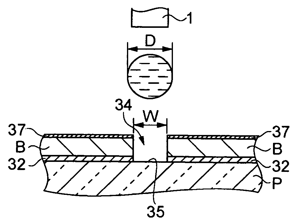
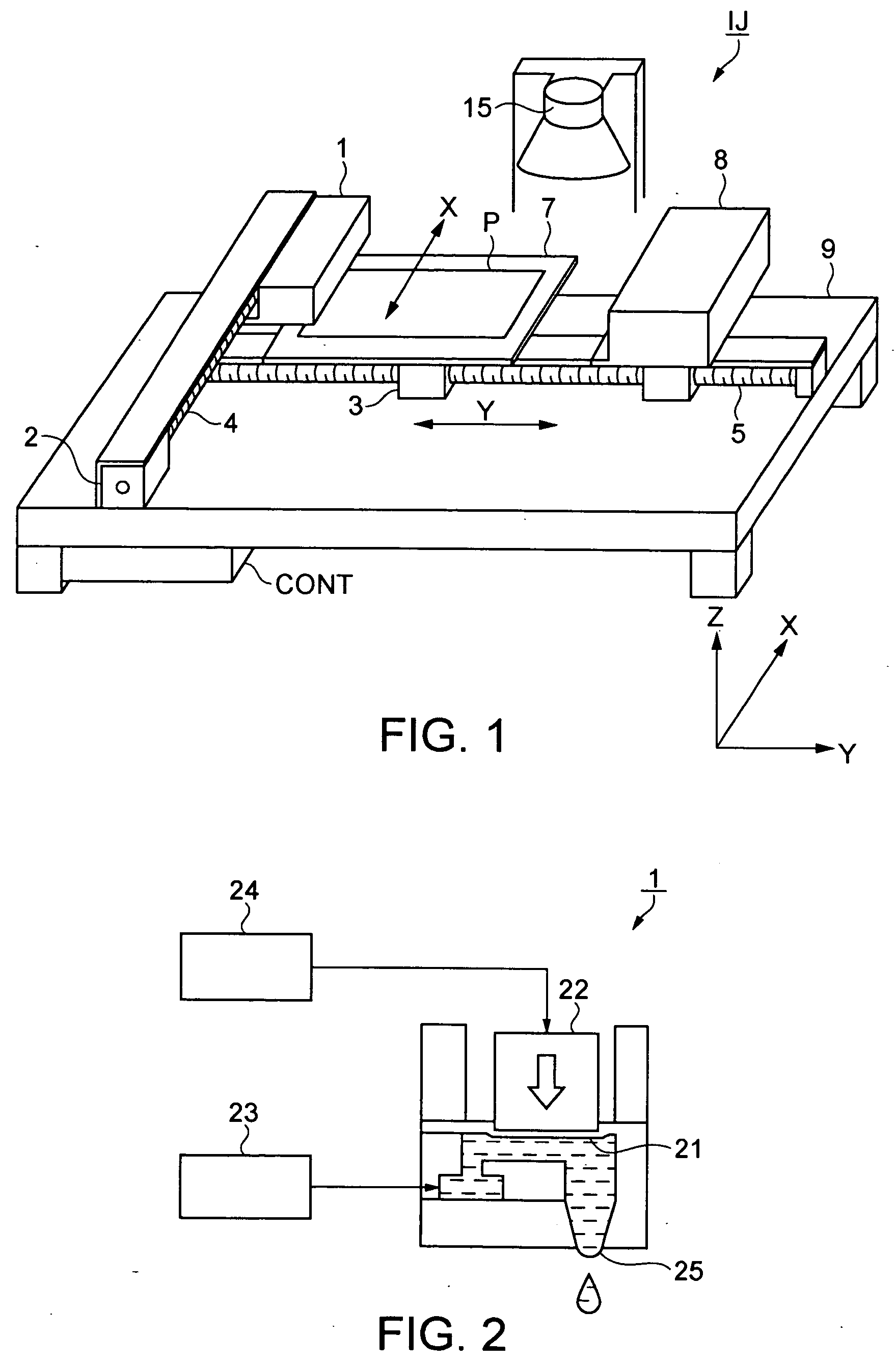
[0052] A thin-film pattern forming method according to a first embodiment of the invention provides a wiring pattern formed by a conductive wiring film on a substrate. The wiring pattern forming method of this embodiment first provides a bank on the substrate so as to define a concave portion surrounded by the bank and having the same planar shape as the thin-film pattern. The method then discharges droplets of ink (functional liquid) for forming a wiring pattern that includes conductive particles from a discharge nozzle included in a droplet discharge head by droplet discharge to the concave portion so as to provide the wiring pattern formed by the conductive wiring film on the substrate. Here, the conductive wiring film corresponds to the first thin film. The wiring pattern corresponds to the thin-film pattern.

[0053] The ink (functional liquid) used as described above will now be described. The ink for forming a wiring pattern, which is a liquid material, is composed of a dispers...

second embodiment

[0100] A thin-film pattern forming method according to a second embodiment of the invention will now be described. In the present embodiment, a method for forming a wiring pattern that forms a circuit wiring further on the wiring pattern formed by the above-described wiring pattern formed in the first embodiment will be described. The droplet discharge method and device used in the present embodiment are fundamentally the same as those employed in the first embodiment.

[0101]FIG. 9 is a flowchart showing an example of the wiring pattern forming method of the present embodiment. According to the wiring pattern forming method of the present embodiment, a bank is provided on the substrate so as to define a concave portion surrounded by the bank and having the same planar shape as the thin-film pattern. Thus, a wiring pattern is formed by providing the ink for forming a wiring pattern, which is described in the first embodiment, in this concave portion and forming a wiring film on the s...

third embodiment

[0126] A liquid crystal display as an example of an electro-optic device according to a third embodiment of the invention will now be described. This liquid crystal display according to the present embodiment includes a TFT having a circuit wiring provided by the thin-film pattern forming method according to the first and second embodiments.

[0127]FIG. 12 is a plan view of the liquid crystal display according to the present embodiment with each component viewed from an opposing substrate. FIG. 13 is a sectional view along line H-H′ of FIG. 12. FIG. 14 is an equivalent circuit view showing each element, wiring, etc. in a plurality of pixels arranged in a matrix in an image display area of the liquid crystal display. FIG. 15 is a partially enlarged view of the liquid crystal display. It should be noted that different scales are used for the layers and members in the drawings, so that the layers and members can be recognized.

[0128] Referring to FIGS. 12 and 13, this liquid crystal dis...


PUM

PropertyMeasurementUnit
contact angleaaaaaaaaaa
diameteraaaaaaaaaa

Abstract

A thin-film pattern forming method that deposits a plurality of thin films on a substrate to form a thin-film pattern, includes: forming a second thin film on the substrate, the second thin film having an affinity for a functional liquid containing a thin-film material that makes up a first thin film; providing lyophobic treatment that makes a surface of the second thin film repellent to the functional liquid; forming a concave portion that defines a pattern shape of the first thin film by removing part of the second thin film; discharging the functional liquid to the concave portion; and forming the first thin film by drying the functional liquid discharged to the concave portion.

Description

BACKGROUND [0001] 1. Technical Field [0002] The present invention relates to a thin-film pattern forming method and a semiconductor device, an electro-optic device and an electronic apparatus that are manufactured by using the thin-film pattern forming method. [0003] 2. Related Art [0004] A related art semiconductor device is provided by depositing a circuit wiring on which a conductive thin film (hereinafter referred to as a wiring film) is placed, a thin film such as an insulating film to cover the circuit wiring, and a semiconductor thin film on a substrate. In order to efficiently form a thin film, the so-called inkjet method is used. The method is to form a thin film by discharging droplets of a functional liquid containing a thin-film material, etc. as a solute from a droplet discharge head and drying the functional liquid that has been landed to remove a solvent. JP-A-11-274671 is an example of related art. In the inkjet method, a concave portion having the same planar shape ...

Claims


Application Information

Patent Timeline
Patent Type & Authority Applications(United States)
IPC IPC(8): H01L21/84
CPCH05K3/125H05K3/1258H05K2201/09909H01L27/1292H05K2203/0568H05K2203/1173H05K2203/013H01L21/288H01L27/1214H01L29/41733H01L29/42384
Inventor MORIYA, KATSUYUKIHIRAI, TOSHIMITSU
Owner SEIKO EPSON CORP
Why Eureka
Try Eureka