Light receiving or light emitting device and itsd production method

a technology of light emitting device and light receiving device, which is applied in the direction of solid-state devices, semiconductor devices, power plants, etc., can solve the problems of increasing the size of the panel, difficult to arrange a plurality of solar cells in the form of a matrix, and complicated solar cell panels, etc., and achieves superior all-purpose utility and easy electrical connection.

Inactive Publication Date: 2006-04-27
SPHELAR POWER
View PDF2 Cites 100 Cited by
  • Summary
  • Abstract
  • Description
  • Claims
  • Application Information

AI Technical Summary

Benefits of technology

[0012] The light receiving or light emitting device of the present invention is a light receiving or light emitting device in which a plurality of particulate semiconductor elements that have a light-to-electricity transducing function or an electricity-to-light transducing function are incorporated lined up in at least one row, this device being characterized in that each of the semiconductor elements has a pair of electrodes that are disposed in spot form on both end parts of the element with the center thereof interposed, a pair of conductive wire members that connect the plurality of semiconductor elements in each row in parallel are provided, and a transparent covering material that covers all of the semiconductor elements and conductive wire members in embedded form is provided. In this light receiving or light emitting device, since a plurality of semiconductor elements that have electrodes formed in spot form on both end parts with the center interposed are lined up in at least a single row, and the semiconductor elements of the respective rows are connected in parallel by a pair of conductive wire members, the electrical connection of numerous semiconductor elements can be accomplished in a simple manner. Since semiconductor elements on which pairs of electrodes are formed are incorporated, there is no need for a complicated process of forming ohmic contacts between the semiconductor elements and the conductive wiring members; the electrodes of the semiconductor elements and the conductive wire members can easily be electrically connected by means of a low melting point metal such as solder or the like. This light receiving or light emitting device can be molded in various shapes, and is deformable as a result of the use of a soft covering material, so that the device is superior in terms of all-purpose utility. If necessary, the various constructions shown below can also be applicable in the present invention.

Problems solved by technology

However, it is not easy to arrange a plurality of the solar cells in the form of a matrix, and to connect these numerous solar cells in a series-parallel connection.
Accordingly, the structure of the solar cell panel becomes complicated, the size of the panel is increased, and the cost of parts and cost of assembly are increased, so that the manufacturing cost of the solar cell panel is increased.
In the case of this solar cell panel, the manufacture of the mesh having a special structure is not easy, and the manufacturing cost is also high.
Accordingly, there are restrictions on the substances that are respectively used to coat the first and second woof filaments, so that it is difficult to lower the manufacturing cost.
The second woof filaments and the p type spherical elements are heated at the time of alloy formation; however, since there is a danger that the donor of the n type diffusion layer formed in the surface will be diffused by heating, there are also restrictions on the substances that can be used as a donor, and control of the heating temperature is also difficult.
However, in the case of such a photo power generating panel, since the numerous spherical power generating elements are connected in parallel, the electromotive force of a single photo power generating panel cannot be increased, and since two printed boards are used, the cost of parts and cost of assembly are high, so that the manufacturing cost of the photo power generating panel is also increased.
Since two printed boards are used, the panel tends to have a high rigidity, so that it is difficult to construct a photo power generating panel with flexibility.
In all of the abovementioned panels, the gap between the electrodes is reduced as the spherical diameter is reduced, so that it is difficult to reduce the size of the panel.
Furthermore, since the spherical light emitting elements do not have independent electrodes, individual testing for defective parts prior to the connection of the elements to the printed wiring is impossible.

Method used


Image

  • Light receiving or light emitting device and itsd production method
  • Light receiving or light emitting device and itsd production method
  • Light receiving or light emitting device and itsd production method

Examples


Embodiment Construction

[0055] An embodiment of the present invention will be described below with reference to the attached drawings.

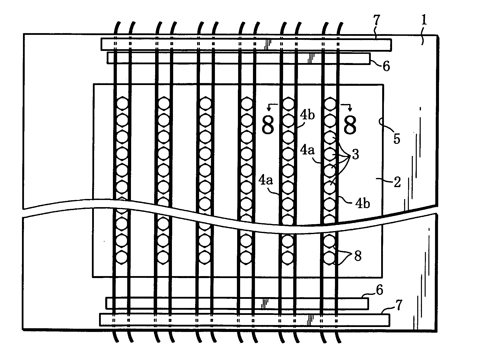
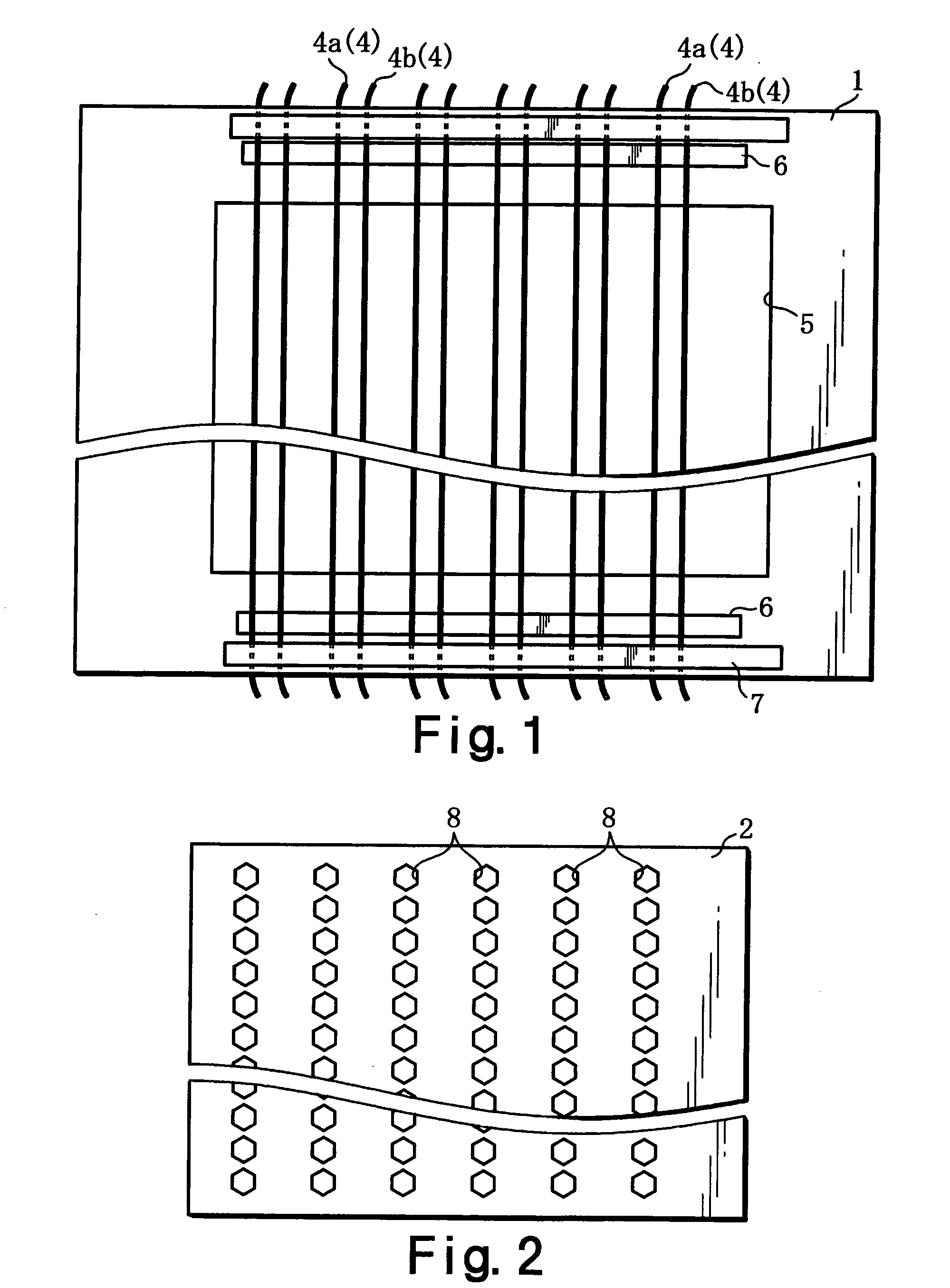
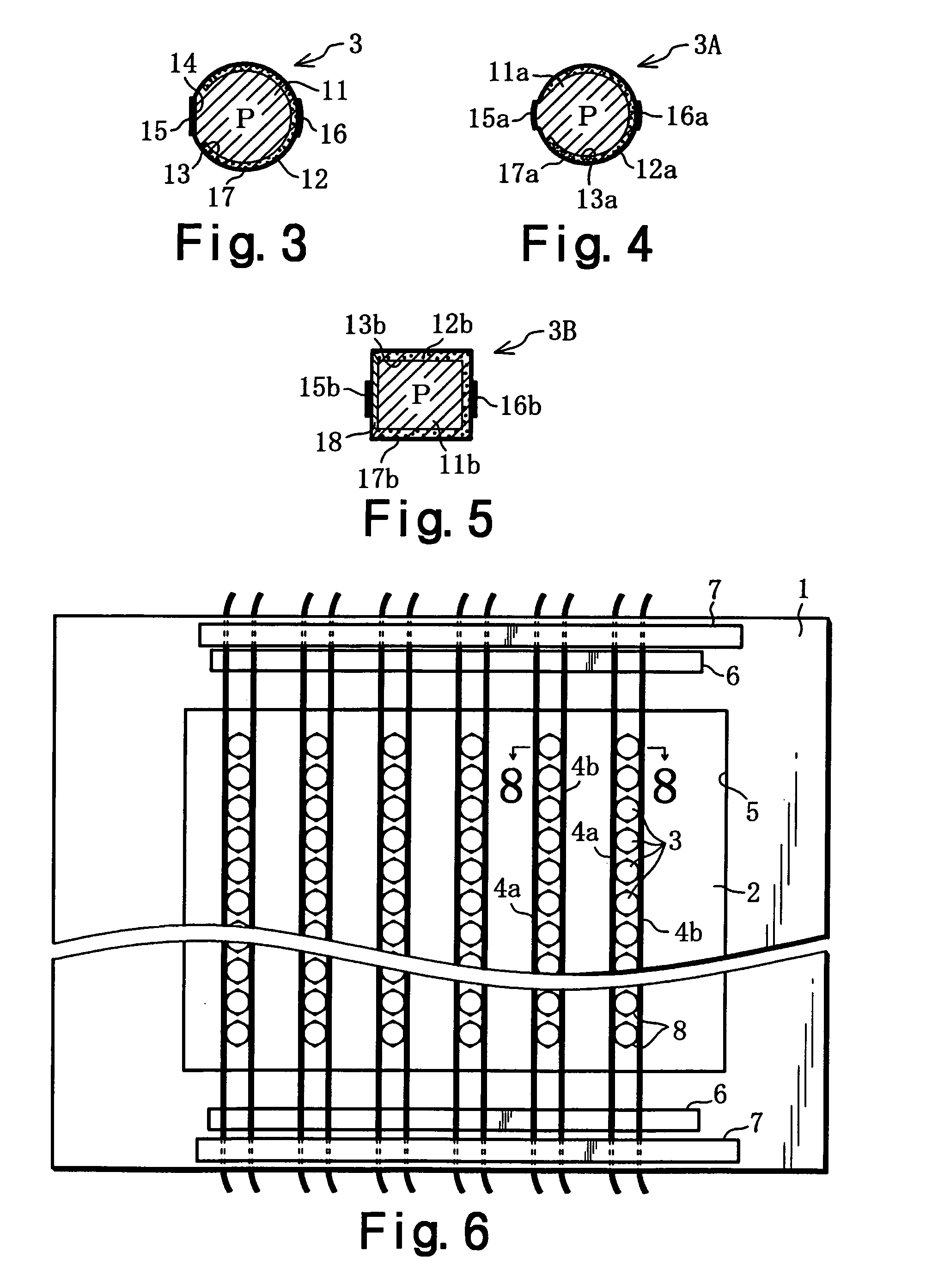
[0056] The present embodiment is one example of a case in which the present invention is applied to a cord-form solar cell used as a light receiving device. First, the method of manufacture and structure of this solar cell will be described. First of all, in a first step, as is shown in FIGS. 1 through 5, a temporary fastening plate 1 to which twelve conductive wire members 4 (positive pole wire members 4a and negative pole wire members 4b) are fastened, a retaining plate 2, and (for example) 120 semiconductor elements 3 (hereafter referred to as “solar cells”), are prepared.

[0057] The temporary fastening plate 1 is a rectangular plate with a thickness of approximately 1 to 2 mm constructed from a hard synthetic resin (e. g., a phenol type or epoxy type synthetic resin) or the like.

[0058] A rectangular opening part 5 that is used to insert the retaining plate 2, and a pai...


PUM


Abstract

A light-receiving device incorporating particulate semiconductor devices (solar cells) having a light-to-electricity transducing function or a light-emitting device incorporating particulate semiconductor devices (light-emitting diodes) having an electricity-to-light transducing function. In a solar cell panel shown, solar cells are arrayed on the same plane in rows. Each row of solar cells are parallel interconnected through positive electrode wires and negative electrode wires, and solar cells of adjoining rows are interconnected in series through a connection part. These solar cells connected in parallel and in series are covered with a transparent covering member, thus forming a panel. These solar cells each have externally exposed positive and negative electrode terminals, and therefore the solar cells can be interconnected in parallel, in series, or in parallel and series. When the conductive wires and the covering member are flexible, the device can be deformable. When the solar cells are replaced with light-emitting diodes, the device can be a light-emitting one.

Description

TECHNICAL FIELD [0001] The present invention relates to a light receiving or light emitting device which can be deformed and simply manufactured by electrically connecting particulate light receiving or light emitting semiconductor elements by means of linear conductive members, and then sealing these elements with synthetic resin, and a method for manufacturing the same. BACKGROUND OF THE INVENTION [0002] Conventional solar cells are constructed with a flat-plate-form structure overall, in which an n type diffusion layer is formed in the surface of a p type semiconductor substrate, a herring-bone-type light receiving surface electrode is formed near the front surface, and a back surface electrode is formed near the back surface. In the case of such flat-plate-form solar cells, when the angle of incidence of sunlight on the solar cell becomes large in the morning or evening, the reflectivity at the surface increases, so that the proportion of the sunlight that enters the interior of...

Claims


Application Information

Patent Timeline
Patent Type & Authority Applications(United States)
IPC IPC(8): H01L21/00H01L25/075H01L31/0352H01L31/042H01L33/32H01L33/56H01L33/58
CPCH01L25/0753H01L31/035281H01L33/20H01L33/24H01L31/0504H01L2924/0002Y02E10/50H01L2924/00
Inventor NAKATA
Owner SPHELAR POWER
Why Eureka
Try Eureka