Tft array substrate, liquid crystal display device, manufacturing methods of tft array substrate and liquid crystal display device, and electronic device

a technology of array substrate and manufacturing method, which is applied in the direction of optics, transistors, instruments, etc., can solve the problems of large work and discarding costs, huge cost of conventional methods, and increased consumption of resists or wiring materials, so as to achieve the effect of greatly reducing the manufacturing process

Inactive Publication Date: 2006-04-27
SHARP KK
View PDF20 Cites 24 Cited by
  • Summary
  • Abstract
  • Description
  • Claims
  • Application Information

AI Technical Summary

Benefits of technology

[0031] More specifically, with the foregoing arrangement, the conductor layer, provided between the semiconductor layer and the source or drain electrode, operates as a diffusion preventing layer for practically preventing diffusion of a component element(s) constituting the source electrode or the drain electrode. Further, the conductor forming layer, which is a previous state of the conductor layer, also operates as the diffusion preventing layer. Here, practical prevention of diffusion refers to an effect that the diffusion amount of the materials is so small even after heat treatment that there is few practical influence of the diffusion to the semiconductor layer.
[0032] With this arrangement, manufacturing processes can be greatly reduced compared to the conventional method for forming a diffusion preventing layer after the semiconductor layer, for example, a method in which the source and drain electrodes are respectively constituted of a diffusion preventing layer and a low electric resistance layer, in this order from the glass substrate.

Problems solved by technology

Accordingly, in order to meet the recent market demand for a larger liquid crystal display device, the conventional method consumes enormous cost, as the TFTs are formed by such a manner with respect to a large-sized substrate.
Furthermore, the demand for a larger substrate brings about greater consumption of resists or wiring material.
Meanwhile, the materials (such as a resist) used in the processing steps for forming the wiring etc., are removed and discarded by etching or removing, since an effective reusing method of those has not yet been realized.
Accordingly, works and costs for the discard are growing bigger with the demand for a larger substrate, as well as environmental burden due to the discarded material.
As described, the conventional manufacturing method of a TFT array substrate, which mainly involves photolithography, requires more manufacturing steps and a greater cost.

Method used


Image

  • Tft array substrate, liquid crystal display device, manufacturing methods of tft array substrate and liquid crystal display device, and electronic device
  • Tft array substrate, liquid crystal display device, manufacturing methods of tft array substrate and liquid crystal display device, and electronic device
  • Tft array substrate, liquid crystal display device, manufacturing methods of tft array substrate and liquid crystal display device, and electronic device

Examples


first embodiment

[0124] One Embodiment of the present invention is described below with reference to FIGS. 1 through 13.

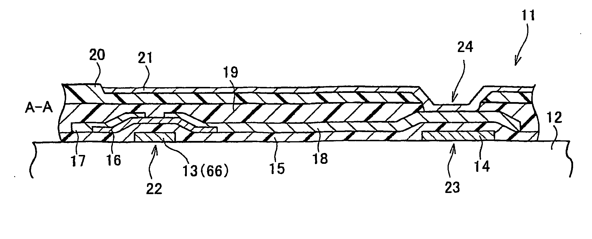
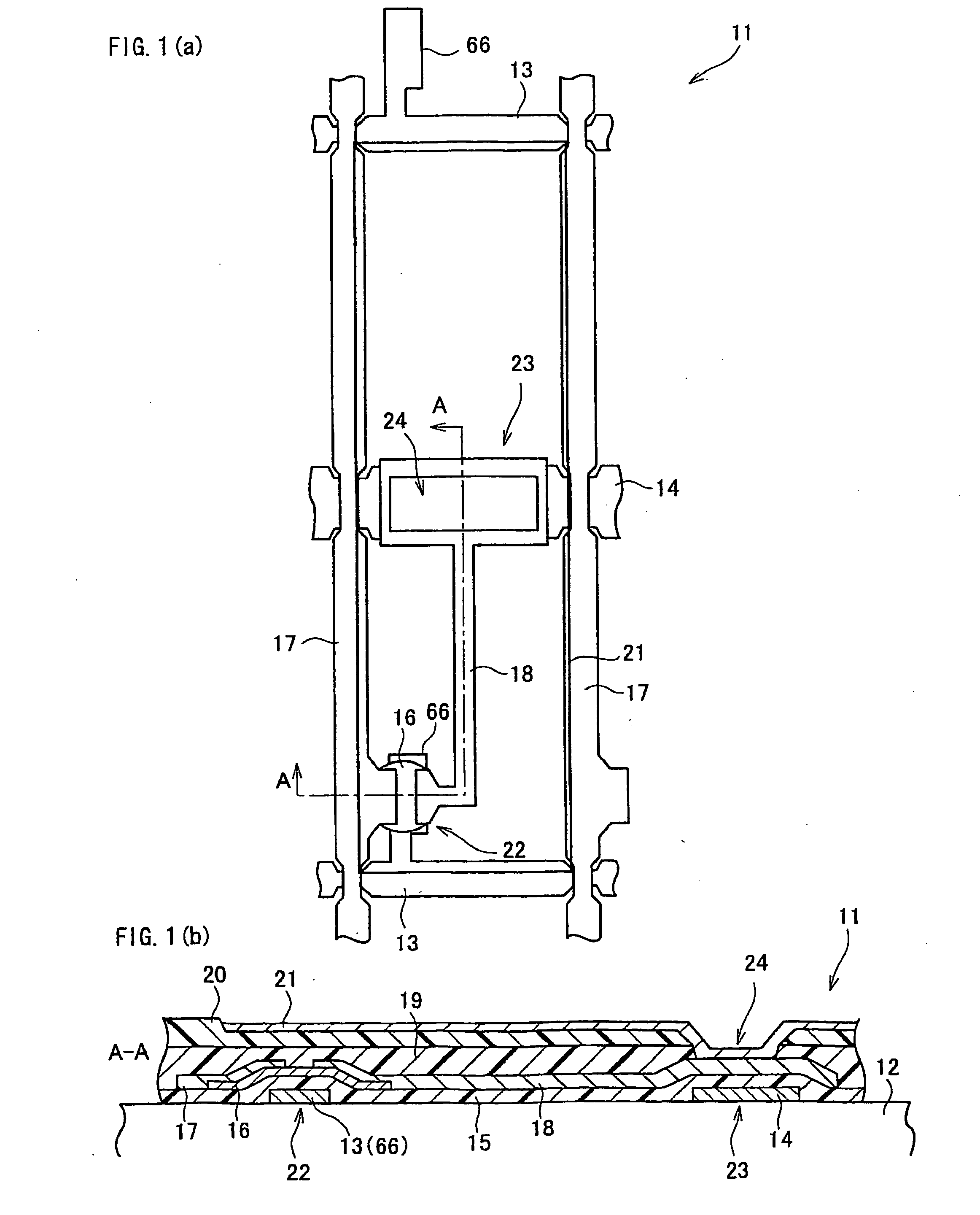
[0125] A liquid crystal display device according to the present Embodiment includes a pixel shown in FIG. 1(a). Note that, FIG. 1(a) is a plan view showing a schematic configuration of a pixel of a TFT array substrate in the liquid crystal display device. Further, FIG. 1(b) is a cross-sectional view, taken along the line A-A of FIG. 1(a).

[0126] As shown in FIGS. 1(a) and 1(b), a TFT array substrate 11 is made of a glass substrate 12 on which a gate electrode 13 and a source electrode 17 are aligned in a matrix manner. A storage capacitor electrode 14 is provided between two adjacent gate electrodes 13.

[0127] As shown in FIG. 1(b), in the TFT array substrate 11, the gate electrode 13 and the storage capacitor electrode 14 are provided on the glass substrate 12 in an area between a TFT section 22 and an storage capacitor section 23; and a gate insulation layer 15 is further provid...

second embodiment

[0201] Another Embodiment of the present invention is described below with reference to FIGS. 15 through 21.

[0202] A liquid crystal display device according to the present Embodiment includes a pixel shown in FIG. 15(a). Note that, FIG. 15(a) is a plan view showing a schematic configuration of a pixel of a TFT array substrate. Further, FIG. 15(b) is a cross-sectional view, taken along the line I-I of FIG. 15(a).

[0203] In the TFT array substrate 11 shown in FIGS. 1(a) and 1(b), the passivation film 19 is formed after the source and drain electrodes 17 and 18, and thereafter, a guide for the pixel electrode is formed by the photosensitive acrylic resin layer 20.

[0204] In manufacturing of a TFT array substrate 81 to be used for a liquid crystal display device according to the present Embodiment, the source electrode 17 and a drain / pixel electrode 82 are formed on the same layer in either of a guide forming process or hydrophilic / hydrophobic process using a photocatalyst, which are c...

third embodiment

[0250] Still another Embodiment of the present invention is described below with reference to FIGS. 33 through 36.

[0251] A liquid crystal display device according to the present Embodiment includes a pixel shown in FIG. 33. FIG. 30 is a plan view showing a schematic configuration of a pixel of a TFT array substrate. Further, this pixel is the same as that shown in FIG. 1(a), which is used for a transmissive liquid crystal display device. For ease of explanation, materials having the equivalent functions as those shown in the drawings pertaining to FIG. 1(a) will be given the same reference symbols, and explanation thereof will be omitted here.

[0252] As shown in FIG. 33, a TFT array substrate 201 according to the present Embodiment has substantially the same configuration as that of the TFT array substrate 11 shown in FIG. 1(a) except for a protrusion electrode 202 extending from an end of the TFT section gate electrode 66, and is provided in contact with the source electrode 17.

[...


PUM

PropertyMeasurementUnit
widthaaaaaaaaaa
temperatureaaaaaaaaaa

Abstract

A TFT array substrate includes a thin film transistor section in which a gate electrode is formed on a substrate, and a semiconductor layer is formed on the gate electrode via a gate insulation layer. The semiconductor layer of this TFT array substrate has a shape formed by dropping a droplet. Accordingly, it is possible to directly forming a semiconductor layer, or a resist layer for forming the semiconductor layer, by dropping a droplet(s). On this account, the present invention allows the use of an inkjet method, thus reducing costs and numbers of manufacturing processes.

Description

TECHNICAL FIELD [0001] The present invention relates to a TFT array substrate; a liquid crystal display device; manufacturing methods of the TFT array substrate and the liquid crystal display device; and an electronic device. BACKGROUND ART [0002] Conventionally, for a liquid crystal display device including a TFT (Thin Film Transistor), a TFT array substrate is manufactured through a series of manufacturing steps, as shown in FIG. 28. More specifically, the manufacturing method of a conventional TFT array substrate is carried out through the steps of depositing a material for gate line, forming the gate line, depositing a gate insulation layer and depositing a semiconductor layer, forming the semiconductor layer, depositing a material for source line and drain line, forming the source line and the drain line, processing a channel section, which exists between the source and the drain electrode on the semiconductor layer, forming a passivation film, processing the passivation film, ...

Claims


Application Information

Patent Timeline
Patent Type & Authority Applications(United States)
IPC IPC(8): H01L29/04H01L21/288G02F1/1368H01L21/3205H01L21/336H01L21/768H01L21/77H01L21/84H01L23/52H01L27/12H01L29/423H01L29/786
CPCH01L27/1292H01L29/42384H01L29/78696H01L29/78633H01L29/66765
Inventor FUJII, AKIYOSHINAKABAYASHI, TAKAYAOCHI, HISAOHARA, TAKAESHISAITOH, YUHICHI
Owner SHARP KK
Why Eureka
Try Eureka