

Manufacturing method for semiconductor light emitting device
a manufacturing method and light-emitting technology, applied in the direction of semiconductor devices, electrical devices, basic electric elements, etc., can solve the problems of difficult to bond the entire face of the transparent substrate uniformly with a high yield, cracks on the wafers, and the inability to proceed to the next step, so as to prevent stress distribution, reduce the contact area of the first wafer and the second wafer, and reduce the bonding area
- Summary
- Abstract
- Description
- Claims
- Application Information
AI Technical Summary
Benefits of technology
Problems solved by technology
Method used
Image

Examples
first embodiment
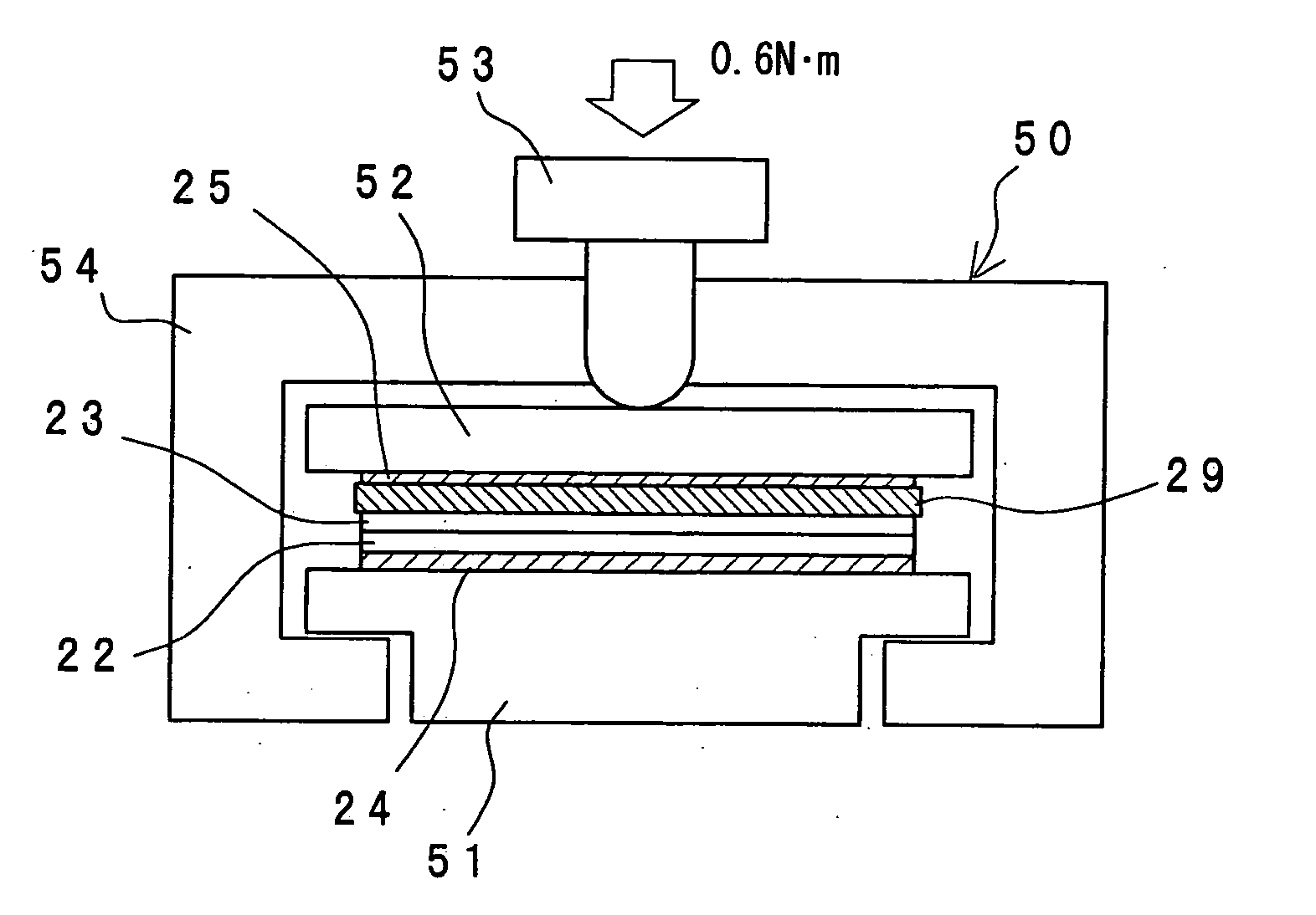
[0073]FIG. 1 is a view showing a bonding step in a manufacturing method for the light emitting diode. The bonding step is a step for bonding a first wafer 22 and a second wafer 23 by applying compressive force to a contact face between the first and second wafers 22 and 23 via a relaxation film 29 as a stress relaxation film constituting a bonding failure prevention structure and also by heating the contact face.
[0074] The first wafer 22 is a wafer having a plurality of semiconductor layers including an emitter layer formed on an n-type GaAs (gallium arsenide) substrate, and the second wafer 23 is a p-type GaP substrate 23 transparent to light from the emitter layer.
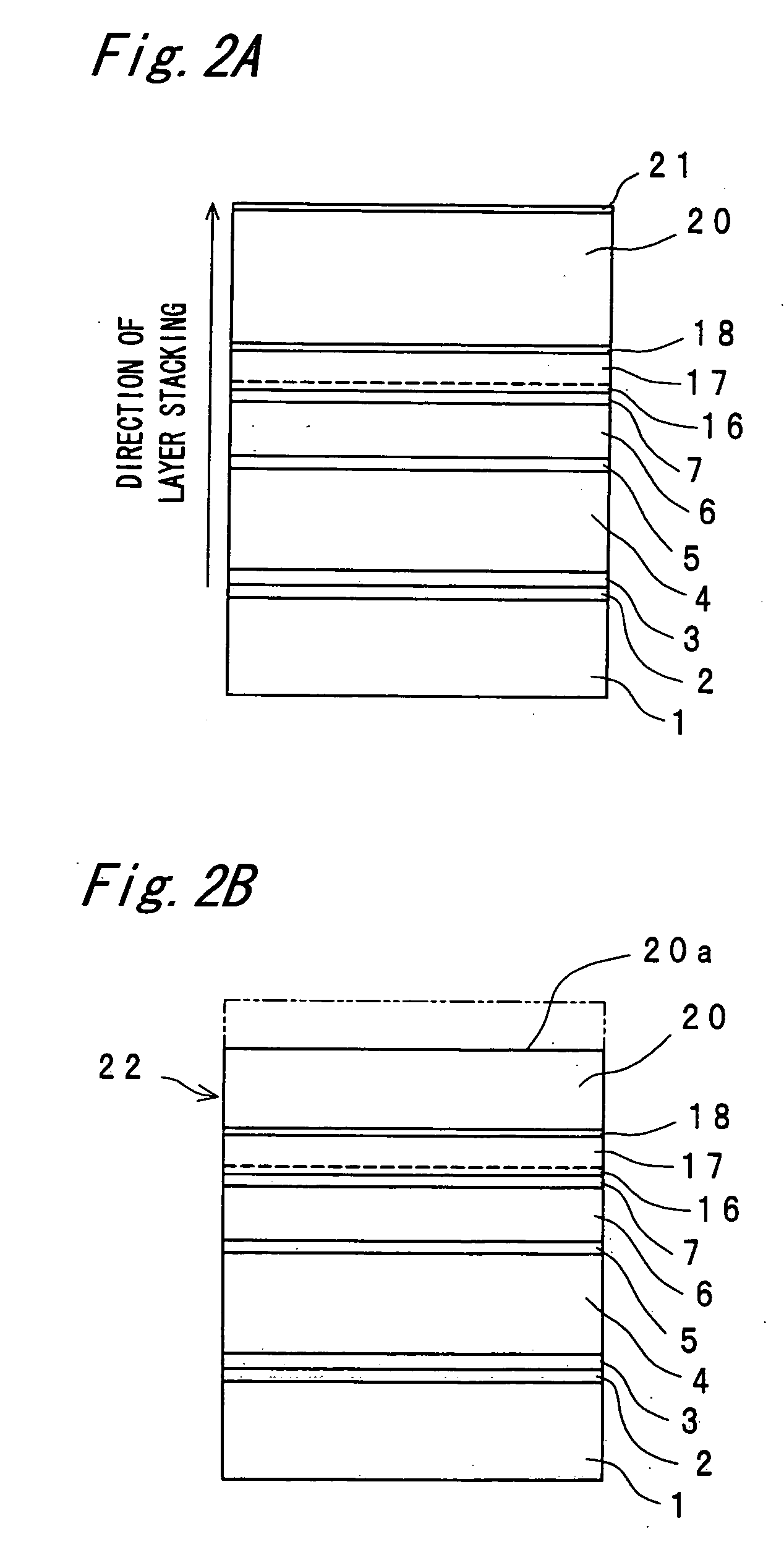
[0075] Hereinbelow, the manufacturing method for the light emitting diode will be described with reference to FIG. 2A to FIG. 2F. It is to be noted that FIG. 2A to FIG. 2E show the portions of the first wafer 22 and the second wafer 23 which should be divided into chips.
[0076] First, as shown in FIG. 2A, on a GaAs sub...
second embodiment
[0095] A manufacturing method for a semiconductor light emitting device in the present embodiment is similar to that in the first embodiment except that the bonding failure prevention structure is a groove formed on the surface of the first wafer 22. In the present embodiment, component members identical to those in the first embodiment are designated by identical reference numerals, and detailed description thereof will be omitted.
[0096] In the present embodiment, after the first wafer 22 shown in FIG. 2B is formed, grooves 61 extending from the surface of the application contact layer 20 to a specified depth are formed in lengthwise and widthwise direction on the surface of the first wafer 22 as shown in FIG. 4. The groove 61, which functions as the bonding failure prevention structure, is formed by dicing. The groove 61 should preferably have a depth of 1 / 20 to ⅓ of the thickness of the first wafer 22. More preferably, the groove 61 should have a depth of 5 to 80 μm. Moreover, t...
third embodiment
[0104] A manufacturing method for a semiconductor light emitting device in the present embodiment is similar to that in the first embodiment except that the bonding failure prevention structure is a first wafer 22 formed to have a specified thickness. In the present embodiment, component members identical to those in the first embodiment are designated by identical reference numerals, and detailed description thereof will be omitted.
[0105] In the present embodiment, after the first wafer 22 shown in FIG. 2B is formed, a surface portion of the first wafer 22 on the GaAs substrate 1 side is grinded by a back grinder as shown in FIG. 6. By this grinding, the thickness of the GaAs substrate 1 of the first wafer 22 is changed from about 350 μm to 250 μm. Consequently, the total thickness of the first wafer 22 becomes about 256 μm. The first wafer 22 formed to have this thickness functions as the bonding failure prevention structure.
[0106] Then, the first wafer 22 having the GaAs substr...
PUM
 Abstract
Description
Claims
Application Information