
Programmable matrix array with chalcogenide material

a chalcogenide material and matrix array technology, applied in the field of programmable matrix arrays, can solve problems such as volatile programmable connection, and achieve the effects of improving efficiency and cost, reducing programming overhead area, and convenient and efficient operation

Active Publication Date: 2006-05-11
OVONYX MEMORY TECH LLC
View PDF21 Cites 107 Cited by
  • Summary
  • Abstract
  • Description
  • Claims
  • Application Information

AI Technical Summary

Benefits of technology

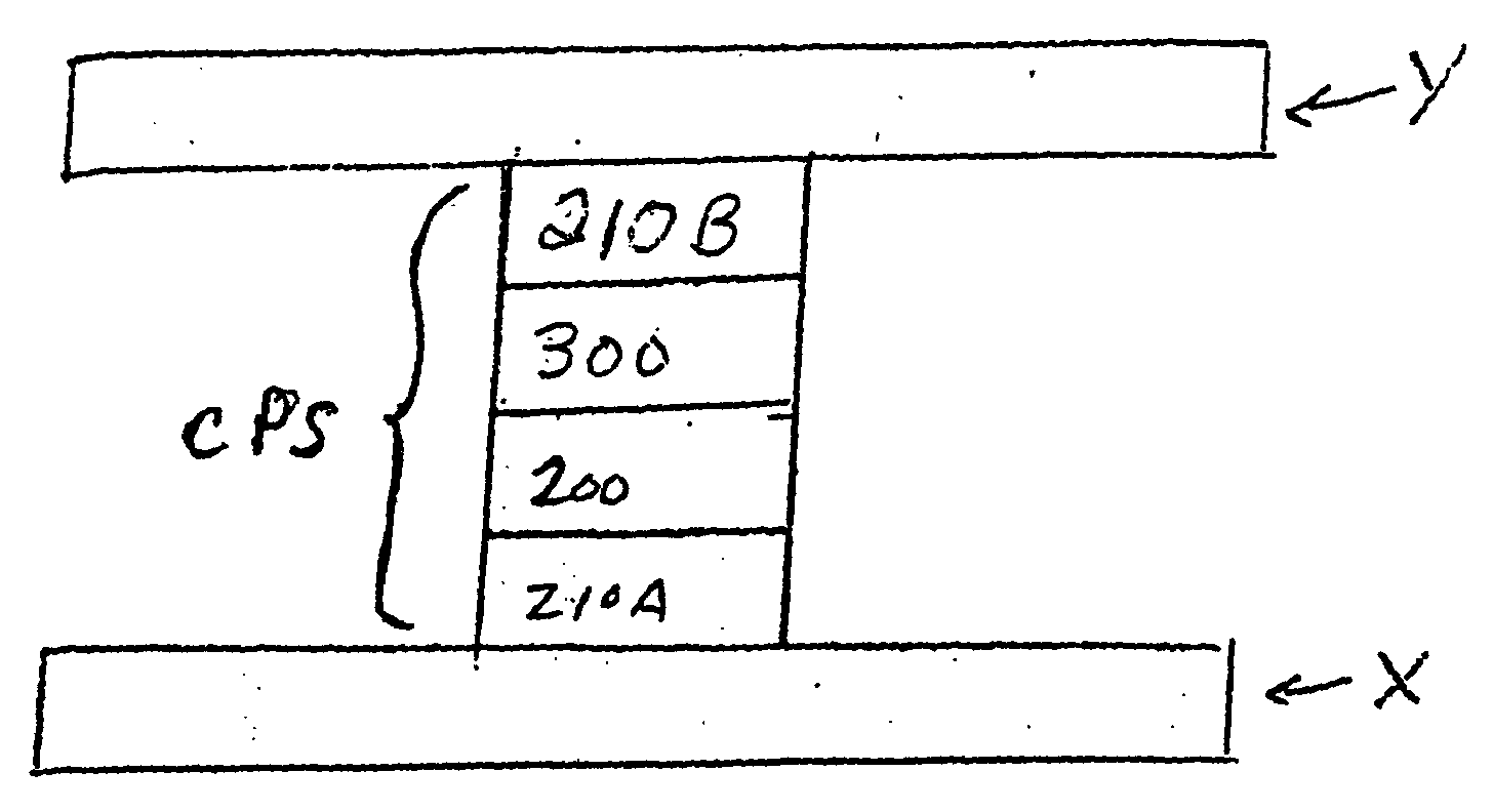
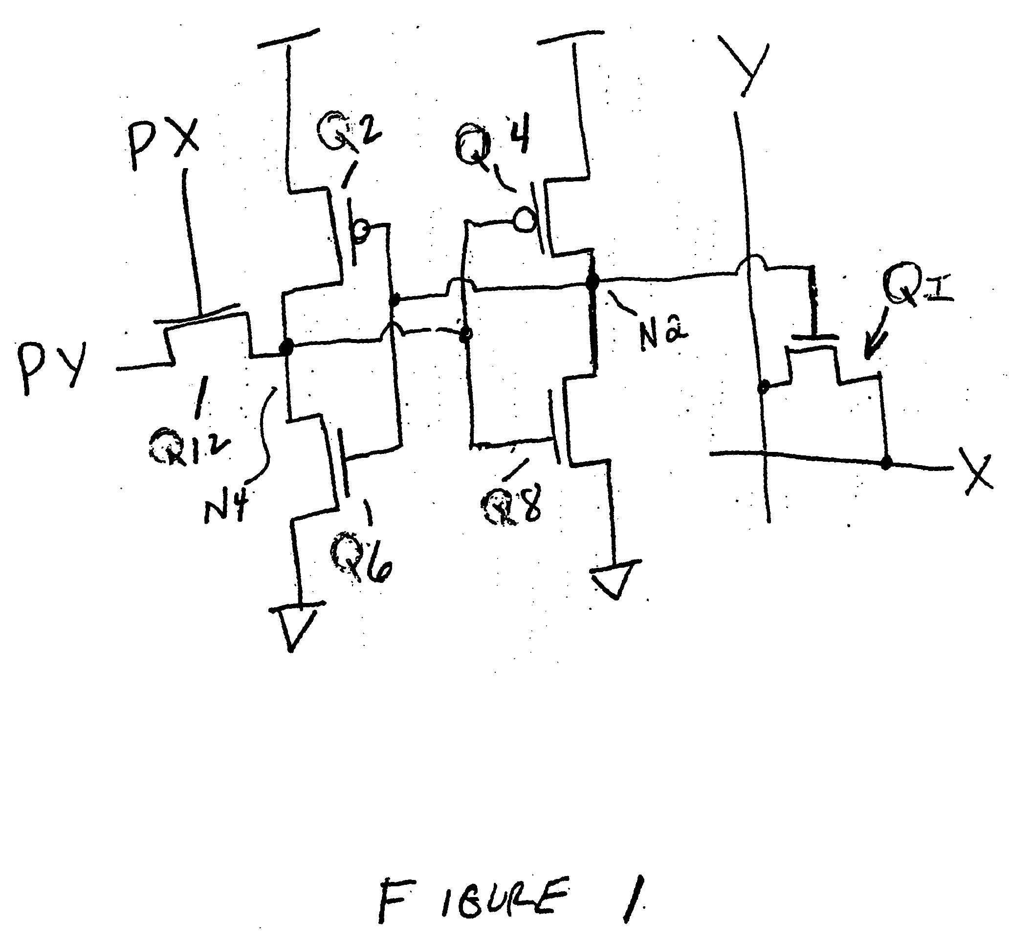
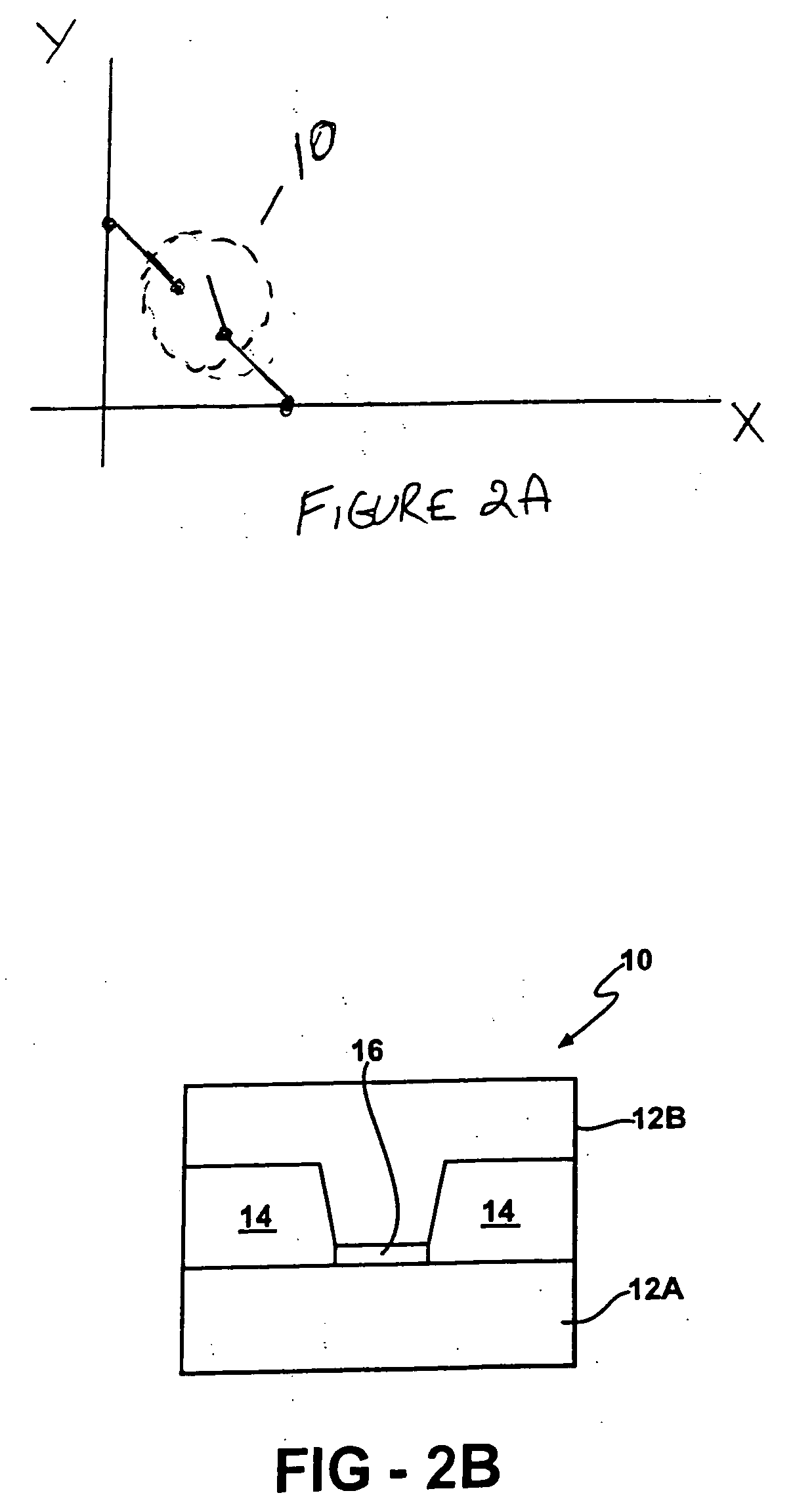
[0034] One aspect of the present invention is a programmable connection comprising a programmable resistance material such as a phase-change material. Such a thin-film programmable connection may be located and fabricated between the intersection of the lines to be coupled by programming. Such a programmable connection may be programmed by the lines to be coupled, without additional programming lines located at or connected to the programmable connection. Instead, the programming control lines and programming devices / drivers may be located anywhere along the interconnect lines, and, for example, more conveniently and efficiently on the ends of the interconnectable lines. Thus the programming devices and lines are shared across more than one programmable connection to reduce programming overhead area for improved efficiency and cost.
[0039] The programmable connection, which may be formed at a cross-point, may be tested by programming the phase-change material to the high resistance reset state and then to the low resistance set state. It is noted, that only those phase-change programmable connections which may potentially be CLOSED (initially or later) would need their breakdown layers penetrated at factory or at initial customer test. For example, if a customer knows that certain cross-points in a general purpose FPLA will probably not be used in certain applications, the breakdown layers of the corresponding programmable connections need not be penetrated. Since the breakdown layer causes the programmable connection to have higher impedance until penetrated, the leakage is thereby reduced while retaining general flexibility at each X-Y interconnection to program it later.
[0040] In sections of the design where lower resistance is desired at a cross-point, such as to drive the heavy capacitance load of a driver device input, several X-Y lines may be wired in parallel. Alternately, a small buffer gate may be permanently wired-in to drive the higher capacitance input. Permanently wired interconnects may also be used for other logic connections in order to reduce the number of programmable connections, thereby further reducing leakage as well as test requirements. Alternately, an SRAM programmable connection (or one or more other existing alternatives) may be wired in parallel with or used on the same chip with the phase-change programmable connections disclosed herein.
[0041] Advantageously, the programmable connection may be made as a thin-film phase-change material, a thin-film threshold switching material or a series combination of phase-change material and threshold switching material (and optionally, a breakdown layer in series therewith) and located between the interconnect conductive layers, preferably reducing chip size and / or freeing up more underlying chip area for logic while still being reversible for improved testability and field repair / changes.

Problems solved by technology

In this case, the programmable connection is volatile and may be reloaded / reprogrammed after turning off the power or after a power glitch where the power is outside its allowed range (high or low).
However, if programmed on at power up, the threshold switch may stay on if the transitions are fast enough and / or adequate leakage is provided to keep the bit on during and after transitions.

Method used


Image

  • Programmable matrix array with chalcogenide material
  • Programmable matrix array with chalcogenide material
  • Programmable matrix array with chalcogenide material

Examples


Embodiment Construction

[0142]FIG. 3A shows an embodiment of an electrically programmable matrix array 100 of the present invention. The matrix array includes a first set of conductive lines X1 through X4 which are also referred to as X lines. The matrix array includes a second set of conductive lines Y1 through Y4 which are also referred to as Y lines. In the example shown there are four X lines and four Y lines. However, more generally, there may be one or more X lines, and there may be one or more Y lines. There may be a plurality of X lines. There may be a plurality of Y lines. Each of the X lines may be adjacent to a segment of a Y line. Each of the X lines may cross (either over or under) each of the Y lines at an angle. The angle may be substantially 90° (that is, substantially perpendicular). The points at which a line crosses over (or under) another or are adjacent to another are referred to as the cross-over points or cross-points.

[0143] The embodiment of the matrix array 100 includes a pluralit...


PUM


Abstract

A memory element, a threshold switching element, or the series combination of a memory element and a threshold switching element may be used for coupling conductive lines in an electrically programmable matrix array. Leakage may be reduced by optionally placing a breakdown layer in series with the phase-change material and / or threshold switching material between the conductive lines. The matrix array may be used in a programmable logic device.

Description

RELATED APPLICATION INFORMATION [0001] This application is a continuation-in-part of U.S. patent application Ser. No. 10 / 983,491, filed on Nov. 8, 2004. This application is also a continuation-in-part of U.S. patent application Ser. No. 11 / 012,571, filed on Dec. 15, 2004, which is a continuation-in-part of U.S. patent application Ser. No. 10 / 983,491, filed on Nov. 8, 2004. This application is also a continuation-in-part of U.S. patent application Ser. No. 11 / 032,792, filed on Jan. 11, 2005. U.S. patent application Ser. No. 10 / 983,491 is hereby incorporated by reference herein. U.S. patent application Ser. No. 11 / 012,571 is hereby incorporated by reference herein. U.S. patent application Ser. No. 11 / 032,792 is hereby incorporated by reference herein.FIELD OF THE INVENTION [0002] The present invention generally relates to programmable integrated circuit devices, and more particularly to a programmable matrix array with programmable connections made with phase-change materials and / or t...

Claims


Application Information

Patent Timeline
IPC IPC(8): H01L29/06
CPCG11C13/0004G11C13/003G11C2213/76H01L27/2427H01L45/04H01L45/1233H01L45/141G11C2213/77H10B63/24H10N70/20H10N70/826H10N70/882
Inventor LOWREY, TYLERPARKINSON, WARDWICKER, GUY
Owner OVONYX MEMORY TECH LLC
Learn More