Semiconductor light-emitting device
a technology of semiconductor devices and light-emitting devices, which is applied in the direction of semiconductor devices, lasers, semiconductor lasers, etc., can solve the problems of increased threshold current, increased tensile distortion, and deterioration of differential efficiency and temperature characteristics, so as to achieve small threshold current and improve tensile distortion , good characteristics
- Summary
- Abstract
- Description
- Claims
- Application Information
AI Technical Summary
Benefits of technology
Problems solved by technology
Method used
Image

Examples
first embodiment
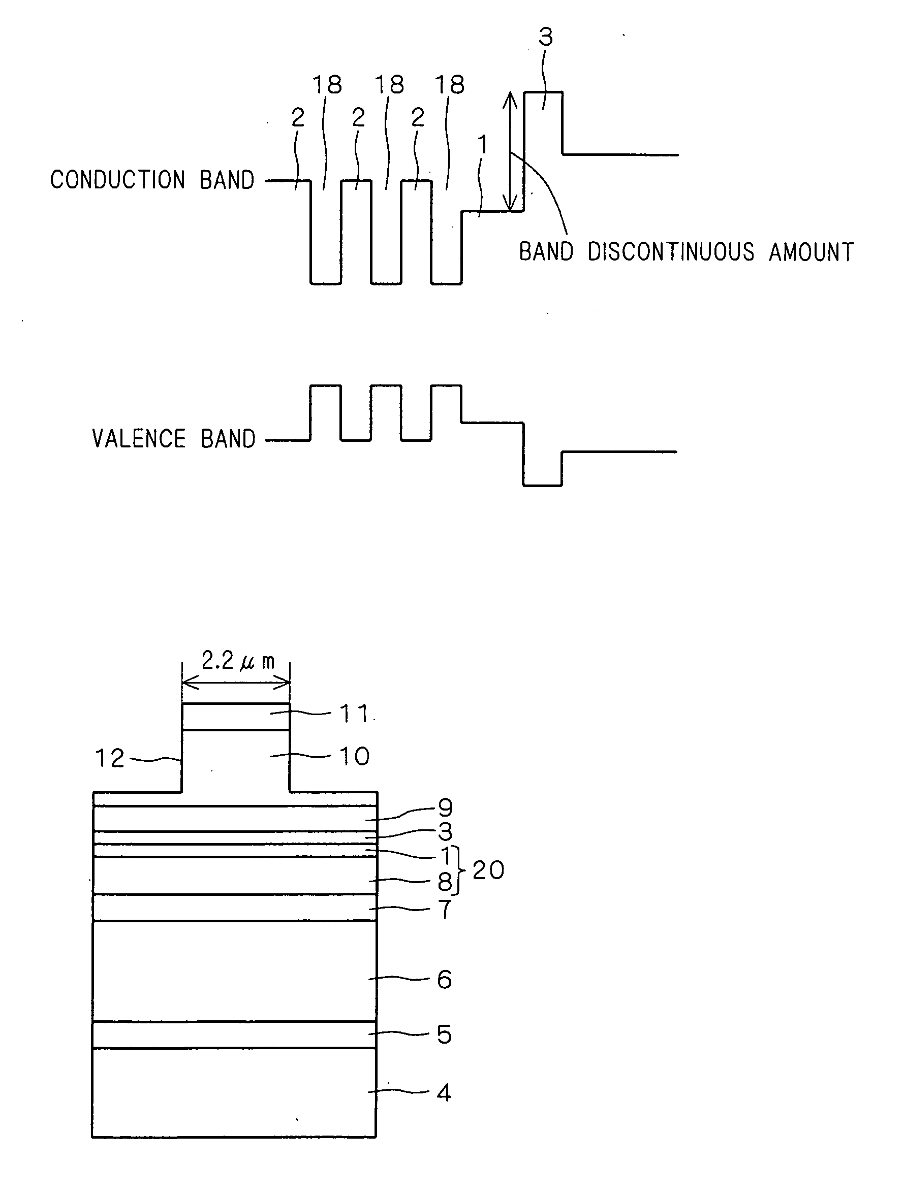
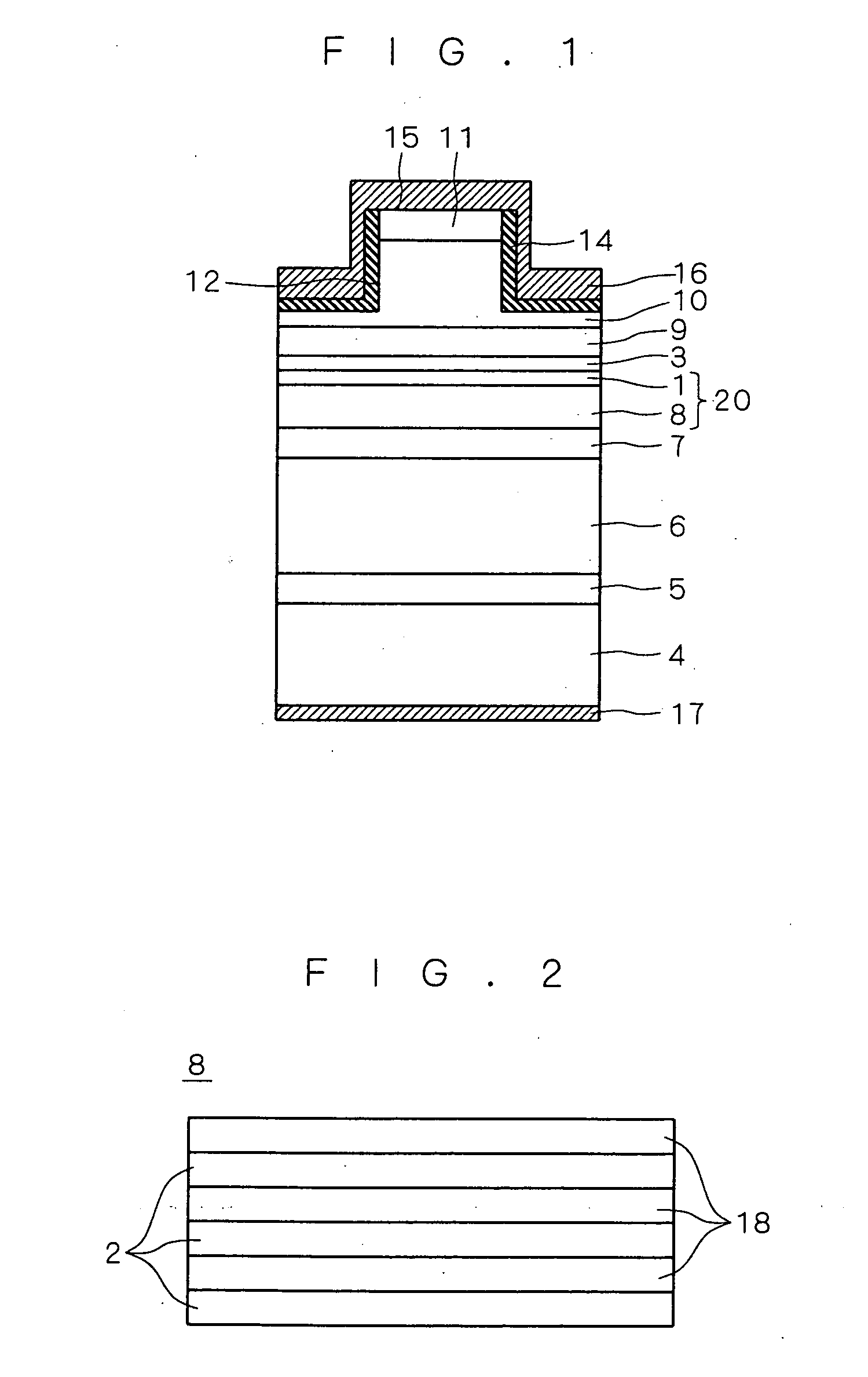
[0035]FIG. 1 is a sectional view showing a configuration of a nitride-based semiconductor laser (semiconductor light-emitting device) according to a first embodiment. This nitride-based semiconductor laser has a ridge structure and an SCH structure.
[0036] As shown in FIG. 1, the nitride-based semiconductor laser according to this embodiment has an n-type GaN buffer layer 5 formed on a Ga surface which is a main surface of a GaN substrate 4. This layer is formed for the purpose of reducing surface undulations on the GaN substrate 4 and laminating the upper layers flatly as much as possible.
[0037] On the n-type GaN buffer layer 5, an n-type AlGaN clad layer (n-type clad layer) 6, an n-type GaN optical guide layer 7 as an n-side guide layer, an active layer 20, a p-type AlGaN electron blocking layer 3 (electron blocking layer, blocking layer), a p-type GaN optical guide layer 9 as a p-side guide layer, a p-type AlGaN clad layer (p-type clad layer) 10, and a p-type GaN contact layer (...
second embodiment
[0084] A nitride-based semiconductor laser according to a second embodiment is similar to the first embodiment, except that the final barrier layer 1 is formed of a plurality of partial final barrier layers 13, 19 (not shown in FIG. 1).
[0085] Herein, the partial final barrier layer 13 is called a first final barrier layer disposed at the n-type clad layer 6 side, and the partial final barrier layer 19 is called a second final barrier layer disposed at the p-type clad layer 6 side.
[0086] The partial final barrier layer 13 has a thickness of, for example, 10 nm, is made of InGaN having an In composition ratio of 0.02, and is formed on the partial active layer 8. On the partial final barrier layer 13, the partial final barrier layer 19 having a thickness of 10 nm and made of InGaN having an In composition ratio of 0.04 is formed.
[0087] Other configuration is same as in the nitride-based semiconductor laser according to the first embodiment, and duplicate explanation is omitted.
[008...
third embodiment
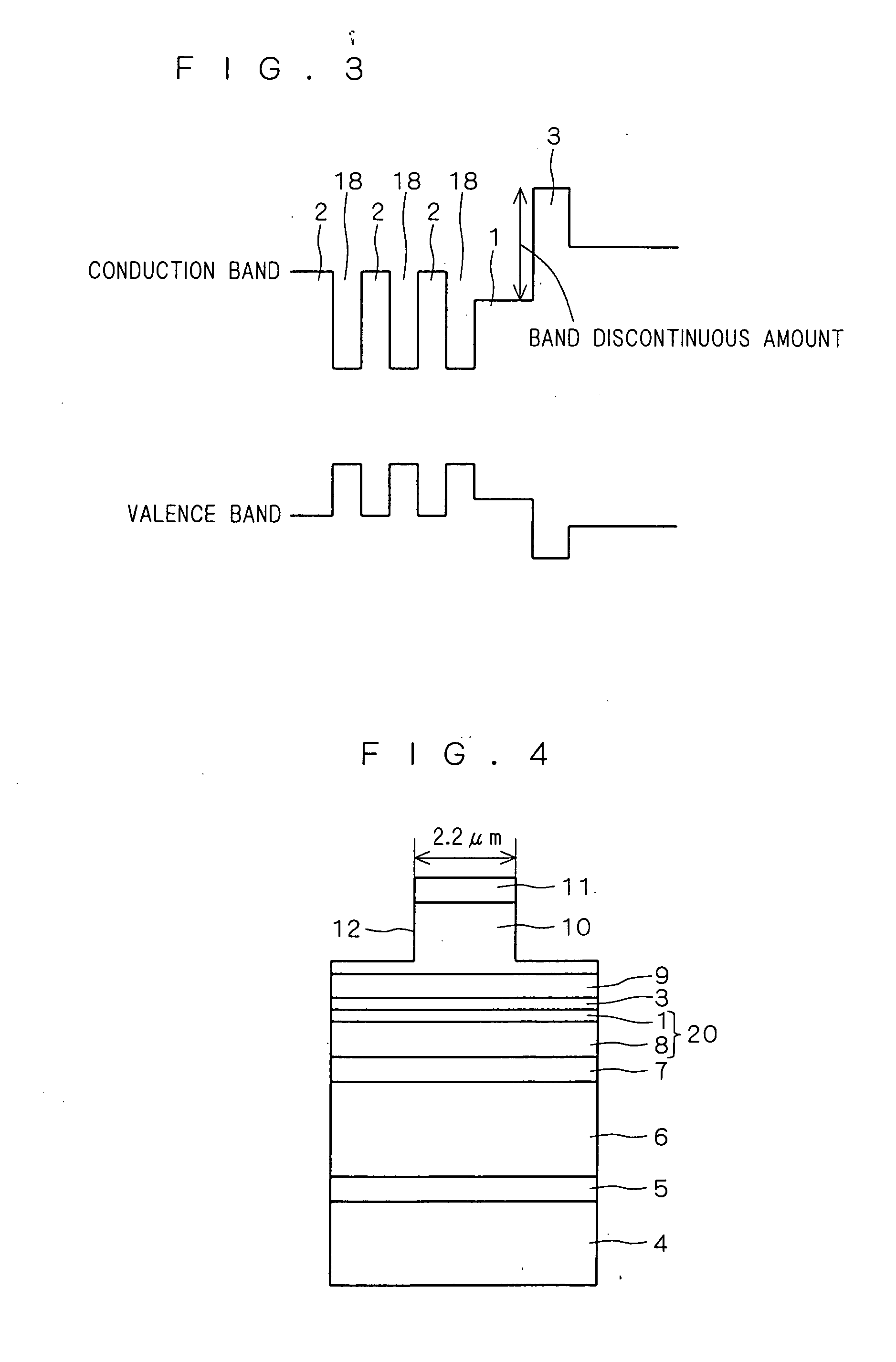
[0101] In a nitride-based semiconductor laser according to a third embodiment, the final barrier layer 1 approaches the electron blocking layer 3 from the side closer to the well layer 18, and is made of InGaN of which In composition ratio increases continuously from 0.02 to 0.04.
[0102] Other configuration is same as in the nitride-based semiconductor laser according to the first embodiment, and duplicate explanation is omitted.
[0103]FIG. 8 is a band diagram in the vicinity of the active layer 20 of the nitride-based semiconductor laser according to this embodiment. As shown in FIG. 8, the band gap of the final barrier layer 1 decreases continuously as approaching the electron blocking layer 3, and at the position contacting with the electron blocking layer 3, the band gap is smaller than the band gap of barrier layer 2.
[0104] A rate of electrons overflowing from electron blocking layer 3 is mostly determined by the band discontinuous amount in a conduction band at the contacting...
PUM
 Abstract
Description
Claims
Application Information
 - R&D
- Intellectual Property
- Life Sciences
- Materials
- Tech Scout
- Unparalleled Data Quality
- Higher Quality Content
- 60% Fewer Hallucinations
Browse by: Latest US Patents, China's latest patents, Technical Efficacy Thesaurus, Application Domain, Technology Topic, Popular Technical Reports.
© 2025 PatSnap. All rights reserved.Legal|Privacy policy|Modern Slavery Act Transparency Statement|Sitemap|About US| Contact US: help@patsnap.com