Amplifier circuit, driving circuit of display apparatus, portable telephone and portable electronic apparatus

a technology of amplifier circuit and driving circuit, which is applied in the direction of amplifiers, amplifiers with semiconductor devices/discharge tubes, instruments, etc., can solve the problems of significant power consumption, significant power consumption on offset correcting operation, and high power consumption, so as to reduce the number of output circuits and reduce the power consumption. , the effect of reducing the number of circuits

Inactive Publication Date: 2006-05-11
VISTA PEAK VENTURES LLC
View PDF10 Cites 12 Cited by
  • Summary
  • Abstract
  • Description
  • Claims
  • Application Information

AI Technical Summary

Benefits of technology

[0034] An object of the present invention is to provide an amplifier circuit capable of realizing the lower power consumption and high-precision output and a controlling method thereof.
[0035] In addition, another object of the present invention is to provide a driving circuit of a display apparatus, controlling method thereof, portable telephone and portable electronic apparatus for realizing the low power consumption, high-precision output and low costs.

Problems solved by technology

In the past, an amplifier circuit for driving a load has a problem that an offset voltage arises due to variations in characteristics of active elements constituting the amplifier circuit.
For that reason, there is a problem that it requires significant power consumption because it is accompanied by charge and discharge of the capacitor in an offset correcting operation.
If the offset correcting operation is performed in each output period, the capacitor for storing the offset voltage must be charged and discharged in each output period, and thus there is a problem that the power consumption on the offset correcting operation is significant even in the case of the amplifier circuit shown in FIG. 47.
In addition, if the offset correcting operation is performed by switch control, there is also a problem that output precision lowers due to influence of capacity coupling occurring on switching.
While it is possible to curb the lowering of the output precision occurring due to the influence of the capacity coupling on switching by increasing the capacity of the capacitor for storing the offset voltage, there is a problem that, if the capacity is increased, the power consumption increases due to the charge and discharge of the capacitor by the offset correcting operation performed in each output period.
While the problems of the amplifier circuits shown in FIGS. 46 and 47 were described above, the other amplifier circuits having offset correction means using the capacitor also have the same problems.
As for the driving circuit in FIG. 49, there are the cases where a plurality of data lines are driven by one gray scale level voltage, and so it is short of the driving capability in case of being used for the large-sized liquid crystal display.
However, the driving circuit shown in FIG. 49 has a problem that, as each of the operational amplifiers 423-1 to 423-n has the offset voltage generated due to variations in characteristics of the transistors constituting the operational amplifiers, variations arise as to precision of the output voltage and display quality is lowered.
For that reason, there is a problem that the required area increases and the cost also increases.
In addition, also in case of using the amplifier circuit shown in FIG. 47 as each of the data line output circuits of the driving circuit shown in FIG. 50, it is necessary to provide the amplifier circuit shown in FIG. 47 to each of m pieces of data lines so that the required area increases and the cost also increases as to the liquid crystal display having a large number of data lines.
Therefore, in the case where each of the data line output circuits of the driving circuit shown in FIG. 50 uses the amplifier circuit shown in FIG. 47, the amount of the offset voltage generated to the operational amplifier 703 in each output period changes as the voltage level of the input signal to each amplifier circuit changes in each output period, and so it is necessary for each amplifier circuit to perform the offset correcting operation in each output period in order to realize the high-precision output in each amplifier circuit and thereby realize the high-precision display and multiple gray scale level display in the liquid crystal display However, there is a problem that, if the offset correcting operation is performed in each output period, the capacitor for storing the offset voltage must be charged and discharged in each output period and thus the power consumption increase.
If the capacity of the capacitor is increased to curb the lowering of the output precision, there is a problem that, the power consumption increases due to the charge and discharge of the capacitor by the offset correcting operation performed in each output period.
However, there are variations in the resistances themselves in the first place, and so the offset voltage of each amplifier cannot be sufficiently reduced according to the size of the resistance even if so attempted, so that sufficient output precision cannot be obtained.

Method used


Image

  • Amplifier circuit, driving circuit of display apparatus, portable telephone and portable electronic apparatus
  • Amplifier circuit, driving circuit of display apparatus, portable telephone and portable electronic apparatus
  • Amplifier circuit, driving circuit of display apparatus, portable telephone and portable electronic apparatus

Examples


first embodiment

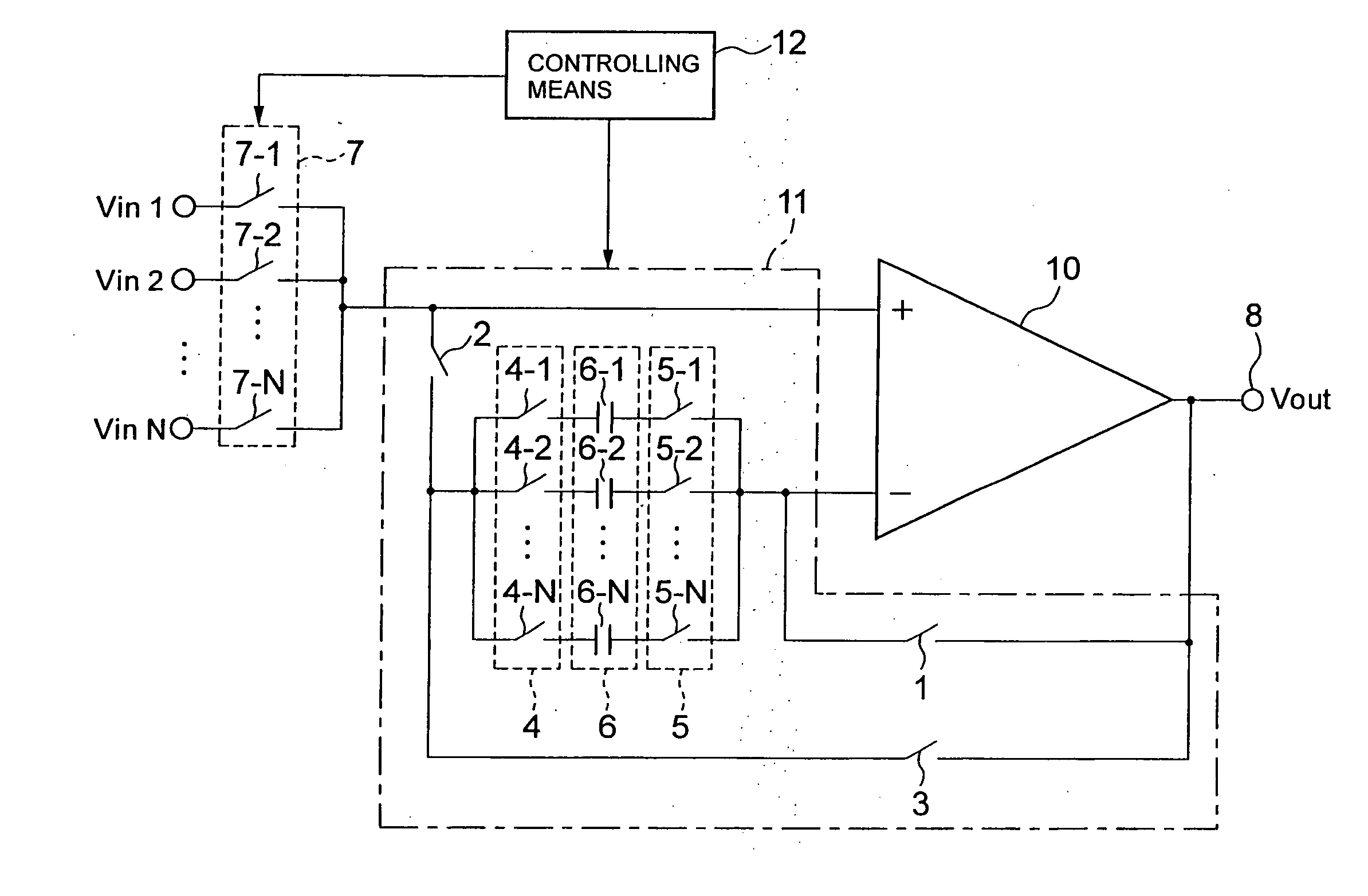
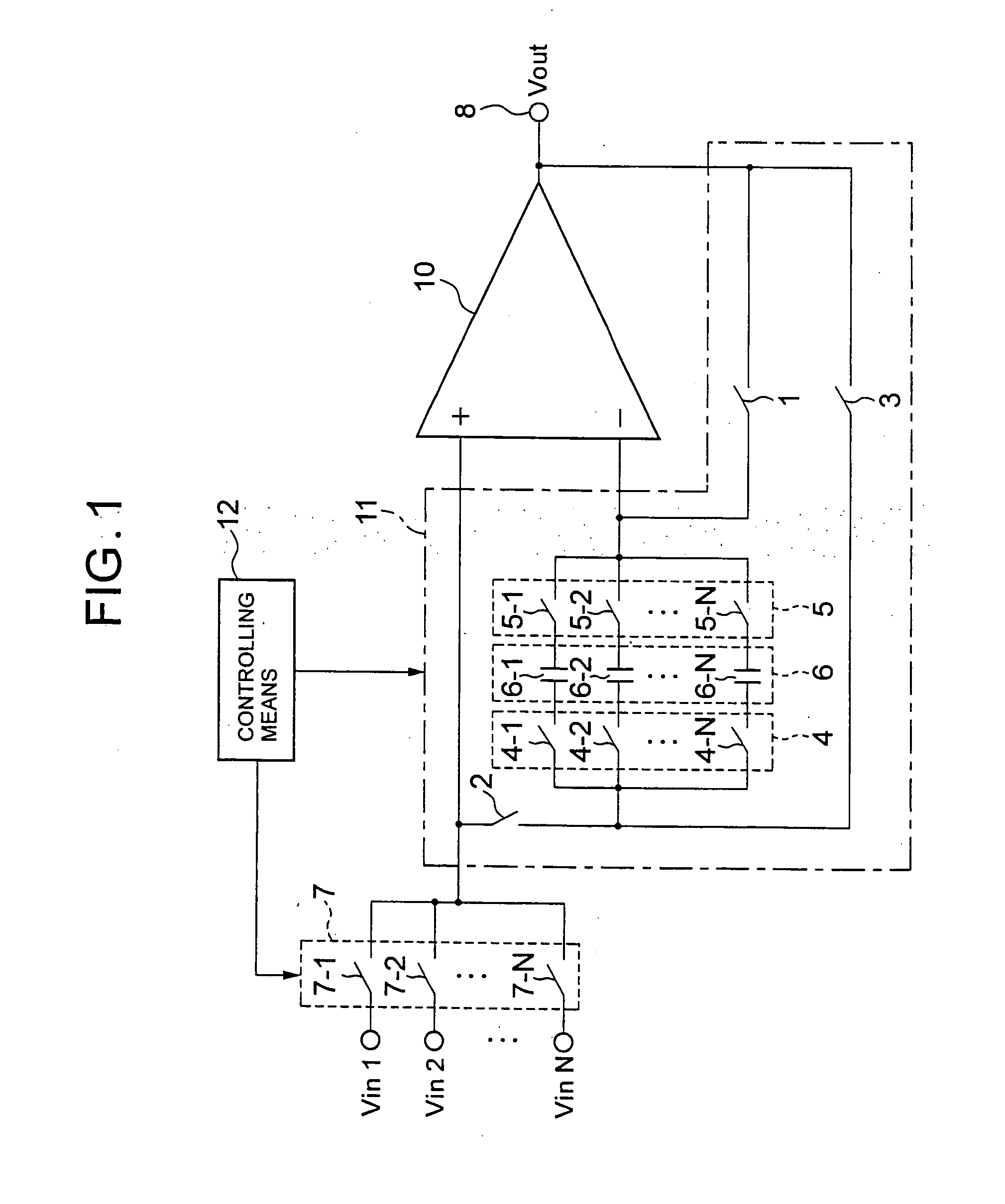
[0103] Hereafter, embodiments of the present invention will be described by using the drawings. FIG. 1 is a diagram showing a configuration of an amplifier circuit according to the present invention. Moreover, equivalent portions are indicated by the same reference numerals in all the drawings shown below.

[0104] In FIG. 1, the amplifier circuit according to the first embodiment of the present invention has input signal selection means 7, an operational amplifier 10, an offset correction circuit 11 and controlling means 12. The input signal selection means 7 has input signal selection switches 7-1 to 7-N connected respectively between N pieces (N is a positive integer) of a circuit input terminal (input terminal of the amplifier circuit) to which N pieces of an input signal (voltage levels of the input signals are Vin1 to VinN respectively) from the outside are supplied and a non-inverting input terminal of the operational amplifier 10.

[0105] The input signal selection means 7 selec...

second embodiment

[0196]FIG. 22 is a diagram showing the configuration of a driving circuit of a display apparatus according to the present invention. The driving circuit shown in FIG. 22 is applicable to the driving circuit of the display apparatus having two polarities, and to be more specific, it is applicable to the driving circuit of the liquid crystal display apparatus having the two polarities which are positive and negative.

[0197] In FIG. 22, the driving circuit of the display apparatus according to the second embodiment of the present invention is comprised of a gray scale level voltage generating means 21 for outputting a plurality of positive gray scale level voltages VP1. VP2, , VPn (n is a positive integer) or a plurality of negative gray scale level voltages VN1, VN2, , VNn, gray scale level output circuits 100-1 to 100-n for amplifying the gray scale level voltages VP1 to VPn or VN1 to VNn from the gray scale level voltage generating means 21, selectors 20-1 to 20-m (m is a positive in...

third embodiment

[0235]FIG. 29 shows the configuration of the driving circuit of the display apparatus according to the present invention. In FIG. 29, the portions equivalent to those in FIG. 22 are indicated by the same symbols. With reference to FIG. 29, each of the gray scale level output circuits 100-1 to 100-n has capacitors 123, 124 connected to the output terminal 8 via switches 151, 152 respectively and the other ends of the capacitors 123, 124 connected to the high-order side power supply VDD and low-order side power supply VSS respectively. Otherwise, the configuration is the same as that in FIG. 1.

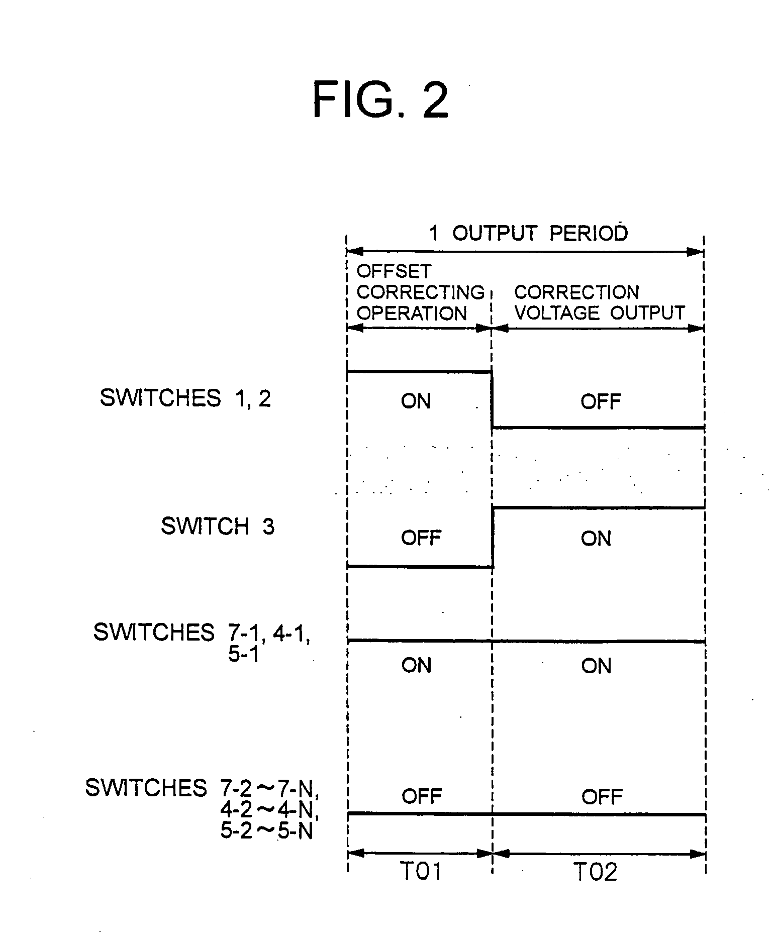
[0236] Next, the operation of the driving circuit of the display apparatus according to the third embodiment of the present invention will be described by referring to the drawings. FIG. 30 is a timing chart showing the operation of each gray scale level output circuit of the driving circuit shown in FIG. 29. Moreover, the switches 1 to 3 and the switches 4-1, 4-2, 5-1, 5-2, 151 and 152 of each ...


PUM


Abstract

To obtain an amplifier circuit capable of realizing low power consumption and high-precision output. A controlling unit controls each switch of an offset correction circuit to select one capacitor associated with a voltage level of an input signal selected by an input signal selection unit, have an offset voltage of an operational amplifier generated according to the voltage level of the input signal stored by the selected capacitor, and correct an output of the operational amplifier by using the offset voltage held by the selected capacitor.

Description

[0001] This application is a division of co-pending application Ser. No. 10 / 358,245, filed on Feb. 5, 2003, the entire contents of which are hereby incorporated by reference.BACKGROUND OF THE INVENTION [0002] 1. Field of the Invention [0003] The present invention relates to an amplifier circuit for driving a load and a controlling method thereof, a driving circuit of a display apparatus and a controlling method thereof a portable telephone and a portable electronic apparatus, and in particular, to the amplifier circuit for correcting an offset voltage of an operational amplifier and a driving circuit of the display apparatus for performing multiple gray scale level display. [0004] 2. Description of the Prior Art [0005] In the past, an amplifier circuit for driving a load has a problem that an offset voltage arises due to variations in characteristics of active elements constituting the amplifier circuit. To solve this problem, various methods of correcting the offset voltage have be...

Claims


Application Information

Patent Timeline
Patent Type & Authority Applications(United States)
IPC IPC(8): G09G5/10G09G3/32G09G3/36H03F3/45
CPCG09G3/3208G09G3/3225G09G3/3291G09G3/3648G09G3/3696G09G2300/0842H03F3/45753H03F3/45977
Inventor NAKAHIRA, YOSHIHIKOTSUCHI, HIROSHI
Owner VISTA PEAK VENTURES LLC
Why Eureka
Try Eureka