Organic thin film transistor array panel and manufacturing method thereof

a technology of organic thin film transistors and array panels, which is applied in the direction of solid-state devices, electric lighting sources, electric light sources, etc., can solve the problems of poor contact characteristic with insulators, deterioration of organic thin film transistor characteristics, and complicated conventional processes for manufacturing organic thin film transistors (tfts), etc., and achieve uniform film quality

Inactive Publication Date: 2006-05-18
SAMSUNG DISPLAY CO LTD
View PDF8 Cites 4 Cited by
  • Summary
  • Abstract
  • Description
  • Claims
  • Application Information

AI Technical Summary

Benefits of technology

[0013] The sputtered ITO layer may include an amorphous ITO layer and may have substantially uniform film quality.

Problems solved by technology

However, conventional processes for manufacturing organic thin film transistors (TFTs), including low molecule semiconductor compounds, can be complicated in that they require a low molecule semiconductor pattern be formed by using a shadow mask and vacuum deposition in order to avoid solvent-induced, in-plane expansion caused by organic solvents.
In addition, the organic semiconductor is prone to change its characteristics or to be damaged by subsequent processing steps, thereby deteriorating the characteristics of organic TFTs.
Although Au has low resistivity and exhibits stable contact with the organic semiconductor, it has a poor contact characteristic with insulator.
In addition, although Mo and Ni have large work function, it is apt to form oxides on their surfaces, which degrade the current characteristics of the TFT.
However, ITO is in poor contact with insulator, in particular, with organic insulator and thus it is difficult to employ ITO signal lines especially in large display devices.

Method used


Image

  • Organic thin film transistor array panel and manufacturing method thereof
  • Organic thin film transistor array panel and manufacturing method thereof
  • Organic thin film transistor array panel and manufacturing method thereof

Examples


Embodiment Construction

[0032] The present invention now will be described more fully hereinafter with reference to the accompanying drawings, in which preferred embodiments of the invention are shown. This invention may, however, be embodied in many different forms and should not be construed as limited to the embodiments set forth herein.

[0033] In the drawings, the thickness of layers and regions are exaggerated for clarity. Like numerals refer to like elements throughout. It will be understood that when an element such as a layer, region or substrate is referred to as being “on” another element, it can be directly on the other element or intervening elements may also be present. In contrast, when an element is referred to as being “directly on” another element, there are no intervening elements present.

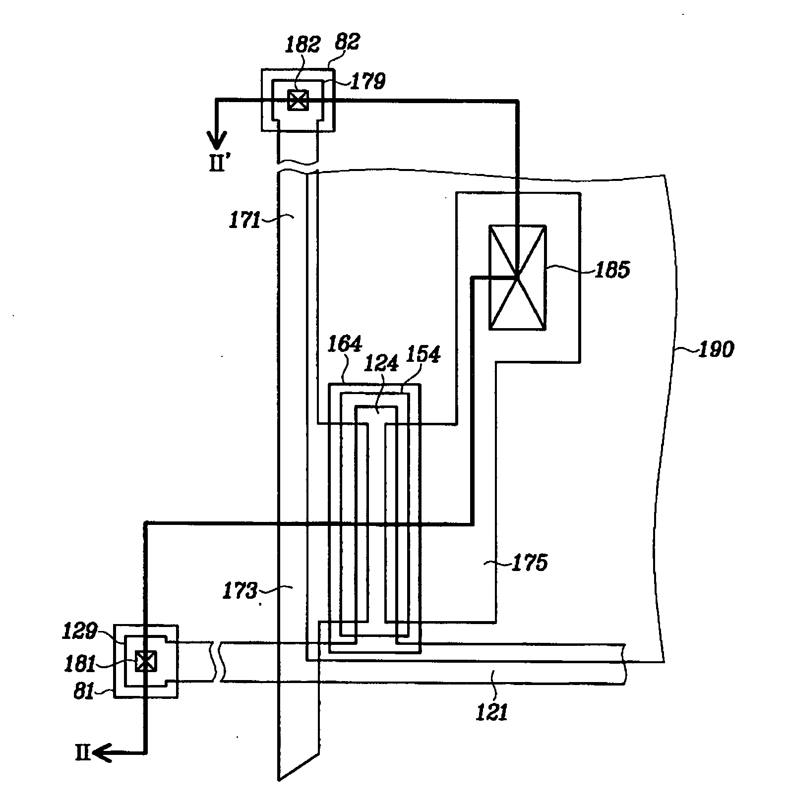
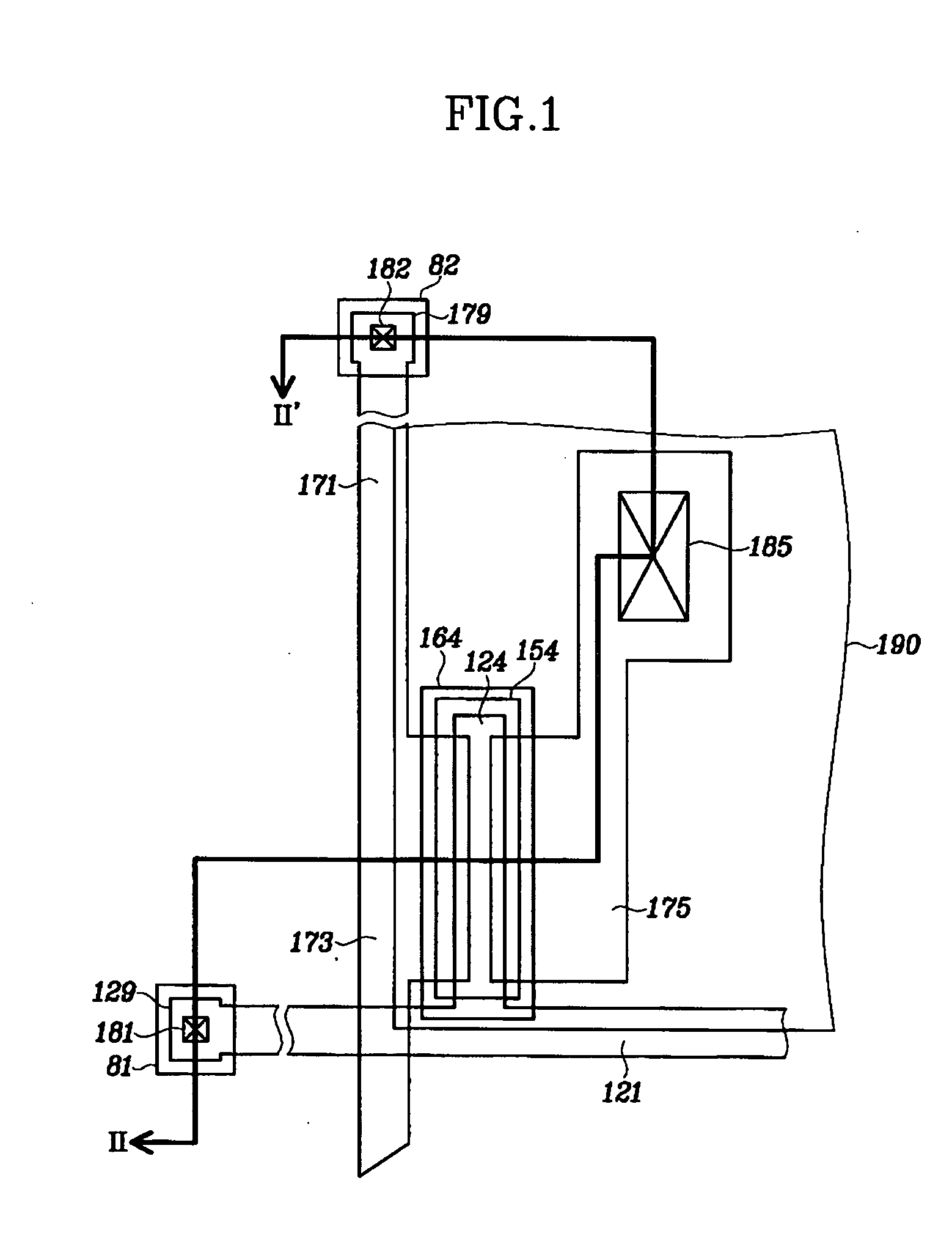
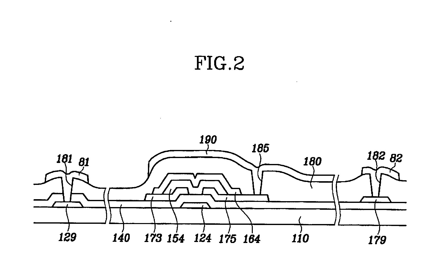
[0034] A TFT array panel according to an embodiment of the present invention will be described with reference to FIGS. 1 and 2.

[0035]FIG. 1 is a layout view of a TFT array panel for an LCD according to...


PUM


Abstract

A method of manufacturing a thin film transistor array panel is provided, the method includes: forming a gate line on a substrate; forming a gate insulating layer on the gate line; depositing an ITO layer at a temperature of about 20-35° C.; etching the ITO layer to form a data line and a drain electrode on the gate insulating layer; and forming an organic semiconductor on the data line, the drain electrode, and the gate insulating layer.

Description

BACKGROUND OF THE INVENTION [0001] (a) Field of the Invention [0002] The present invention relates to a thin film transistor array panel and a manufacturing method thereof, and in particular, to an organic thin film transistor array panel and a manufacturing method thereof. [0003] (b) Description of Related Art [0004] Electric field effect transistors including organic semiconductors have been vigorously researched as driving devices for next generation display devices. Organic semiconductors may be classified into low molecule compounds such as oligothiophene, pentacene, phthalocyanine, and C6O; and high molecule compounds such as polythiophene and polythienylenevinylene. The low molecule semiconductors have a high mobility in a range of about 0.05-1.5 msV, and superior on / off current ratios. [0005] However, conventional processes for manufacturing organic thin film transistors (TFTs), including low molecule semiconductor compounds, can be complicated in that they require a low mol...

Claims


Application Information

Patent Timeline
Patent Type & Authority Applications(United States)
IPC IPC(8): H01L21/00H01L21/84
CPCH01L27/3244H01L51/0545H01L51/105H10K59/12H10K10/84H10K10/466H05B33/26H05B33/10
Inventor RYU, MIN-SEONGSEO, JONG-HYUNHONG, MUN-PYO
Owner SAMSUNG DISPLAY CO LTD
Why Eureka
Try Eureka