Semiconductor integrated circuit devices having single crystalline thin film transistors and methods of fabricating the same

a technology of integrated circuit devices and thin film transistors, which is applied in the direction of semiconductor devices, basic electric elements, electrical equipment, etc., can solve the problems of low integration density of bulk cmos sram cells, weak latch-up immunity, and difficult to transform the body layer into a single crystalline silicon layer. , to achieve the electrical characteristics of bulk transistors, the difficulty of forming the body layer

Inactive Publication Date: 2006-05-18
SAMSUNG ELECTRONICS CO LTD
View PDF12 Cites 20 Cited by
  • Summary
  • Abstract
  • Description
  • Claims
  • Application Information

AI Technical Summary

Problems solved by technology

However, the bulk CMOS SRAM cell has low integration density and weak latch-up immunity as compared to the TFT SRAM cell.
That is, it is difficult to transform the body layer into a perfect single crystalline silicon layer.
As a result, it is difficult to form the TFT having the electrical characteristics of the bulk transistor.

Method used


Image

  • Semiconductor integrated circuit devices having single crystalline thin film transistors and methods of fabricating the same
  • Semiconductor integrated circuit devices having single crystalline thin film transistors and methods of fabricating the same
  • Semiconductor integrated circuit devices having single crystalline thin film transistors and methods of fabricating the same

Examples


Embodiment Construction

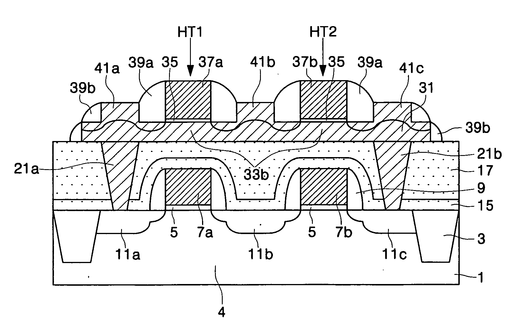
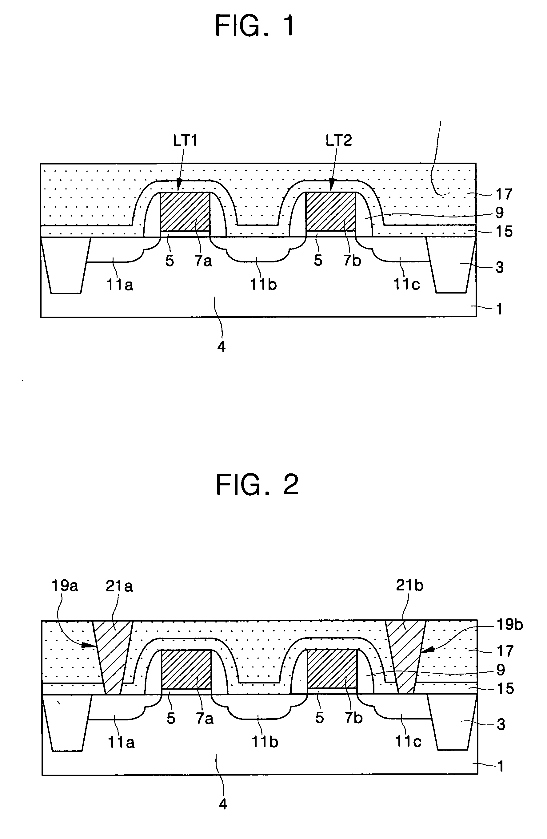
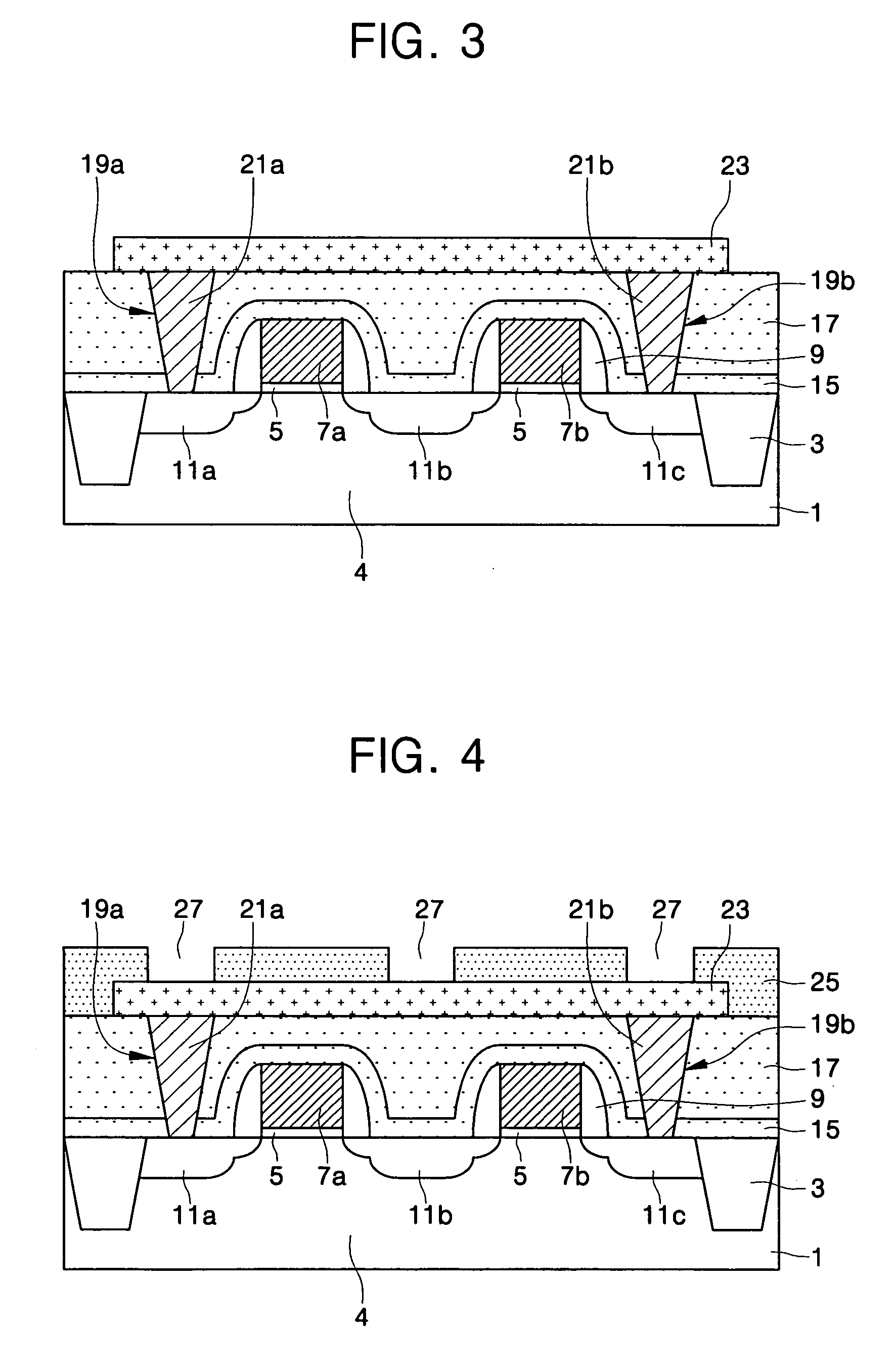
[0032] FIGS. 1 to 8 are cross-sectional views illustrating methods of fabricating semiconductor integrated circuit devices in accordance with embodiments of the present invention.

[0033] Referring to FIG. 1, an isolation layer 3 is formed in a predetermined region of a semiconductor substrate 1 such as a silicon substrate to define an active region 4. A lower gate insulating layer 5 and a lower gate material layer are sequentially formed on the active region 4. The lower gate material layer may be formed by sequentially stacking a gate conductive layer and a gate capping layer. Alternatively, the lower gate material layer may be formed of only the gate conductive layer. The gate conductive layer may be formed of a doped polysilicon layer or a metal layer, and the gate capping layer may be formed of an insulating layer such as a silicon oxide layer or a silicon nitride layer. The lower gate material layer is patterned to form first and second lower gate patterns 7a and 7b. In this ca...


PUM


Abstract

Semiconductor integrated circuit devices having single crystalline thin film transistors and methods of fabricating the same are provided. The semiconductor integrated circuit devices include an interlayer insulating layer formed on a semiconductor substrate and a single crystalline semiconductor plug penetrating the interlayer insulating layer. A single crystalline semiconductor body pattern is provided on the interlayer insulating layer. The single crystalline semiconductor body pattern has an elevated region and contacts the single crystalline semiconductor plug. The method of forming the single crystalline semiconductor body pattern having the elevated region includes forming a sacrificial layer pattern covering the single crystalline semiconductor plug on the interlayer insulating layer. A capping layer is formed to cover the sacrificial layer pattern and the interlayer insulating layer, and the capping layer is patterned to form an opening which exposes a portion of the sacrificial layer pattern. Subsequently, the sacrificial layer pattern is selectively removed to form a cavity in the capping layer, and a planarized single crystalline semiconductor body pattern is formed to fill the cavity and the opening.

Description

CROSS-REFERENCE TO RELATED APPLICATION [0001] This application claims the benefit of Korean Patent Application No. 10-2004-0093742, filed Nov. 16, 2004, the contents of which are hereby incorporated herein by reference in their entirety. BACKGROUND OF THE INVENTION [0002] 1. Field of the Invention [0003] The present invention relates to semiconductor devices and methods of fabricating the same and, more particularly, to semiconductor integrated circuit devices having single crystalline thin film transistors and methods of fabricating the same. [0004] 2. Description of the Related Art [0005] Static random access memories (SRAMs) of semiconductor integrated circuit devices have advantages of low power consumption and fast operating speed as compared to dynamic RAMs (DRAMs). The SRAMs are thus widely used in portable appliances or cache memory devices of computers. [0006] Unit cells of SRAM devices are typically classified into two categories. One is a high load resistor SRAM cell empl...

Claims


Application Information

Patent Timeline
Patent Type & Authority Applications(United States)
IPC IPC(8): H01L29/94
CPCH01L21/8221H01L27/0688H10B10/00
Inventor KIM, SUNG-JINJUNG, SOON-MOONCHO, WON-SEOKJANG, JAE-HOONKIM, JONG-HYUKKWAK, KUN-HOLIM, HOON
Owner SAMSUNG ELECTRONICS CO LTD
Why Eureka
Try Eureka