Method of fabricating T-type gate

a gate and t-type technology, applied in the direction of basic electric elements, electrical equipment, semiconductor devices, etc., can solve the problems of many steps, difficult to adapt the photoresist layer on the insulating layer rather than the metal layer, and the device cannot be easily manufactured, so as to reduce the manufacturing cost and enhance the yield

Inactive Publication Date: 2006-11-28
ELECTRONICS & TELECOMM RES INST
View PDF5 Cites 4 Cited by
  • Summary
  • Abstract
  • Description
  • Claims
  • Application Information

AI Technical Summary

Benefits of technology

[0009]The present invention is directed to a method of fabricating a T-type gate capable of facilitating a compound semiconductor device manufacturing process, enhancing the yield, and reducing the manufacturing cost by forming two kinds of patterns from one kind of photoresist layer using electron beam and photolithography technologies and by interposing a blocking layer between upper and lower photoresist layers for reversing the patterns.

Problems solved by technology

The process has difficulties in implementing the devices since it is difficult to realize a fine pattern, the process becomes complicated, and the device cannot be easily manufactured.
However, in forming the fine pattern using the electron beams, it is more difficult to adapt the photoresist layer on an insulating layers rather than a metal layer due to an electron charging effect.
As described above, according to the conventional method, many steps are required and it is difficult to form the fine pattern.
Also, a metal lift-off process cannot be smoothly performed since the metal is not deposited with a low step coverage required.

Method used


Image

  • Method of fabricating T-type gate
  • Method of fabricating T-type gate
  • Method of fabricating T-type gate

Examples


Embodiment Construction

[0016]The present invention will now be described more fully hereinafter with reference to the accompanying drawings, in which exemplary embodiments of the invention are shown. This invention may, however, be embodied in different forms and should not be construed as limited to the embodiments set forth herein. Rather, these embodiments are provided so that this disclosure is thorough and complete and fully conveys the scope of the invention to those skilled in the art.

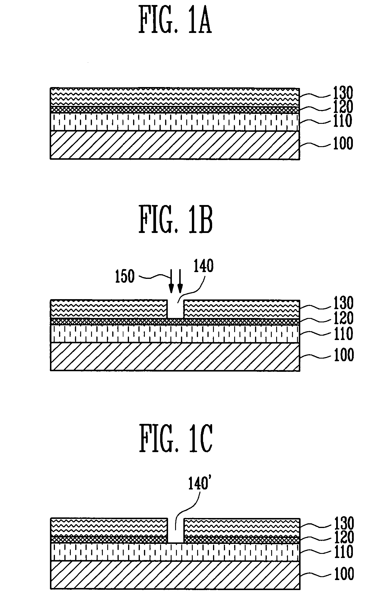
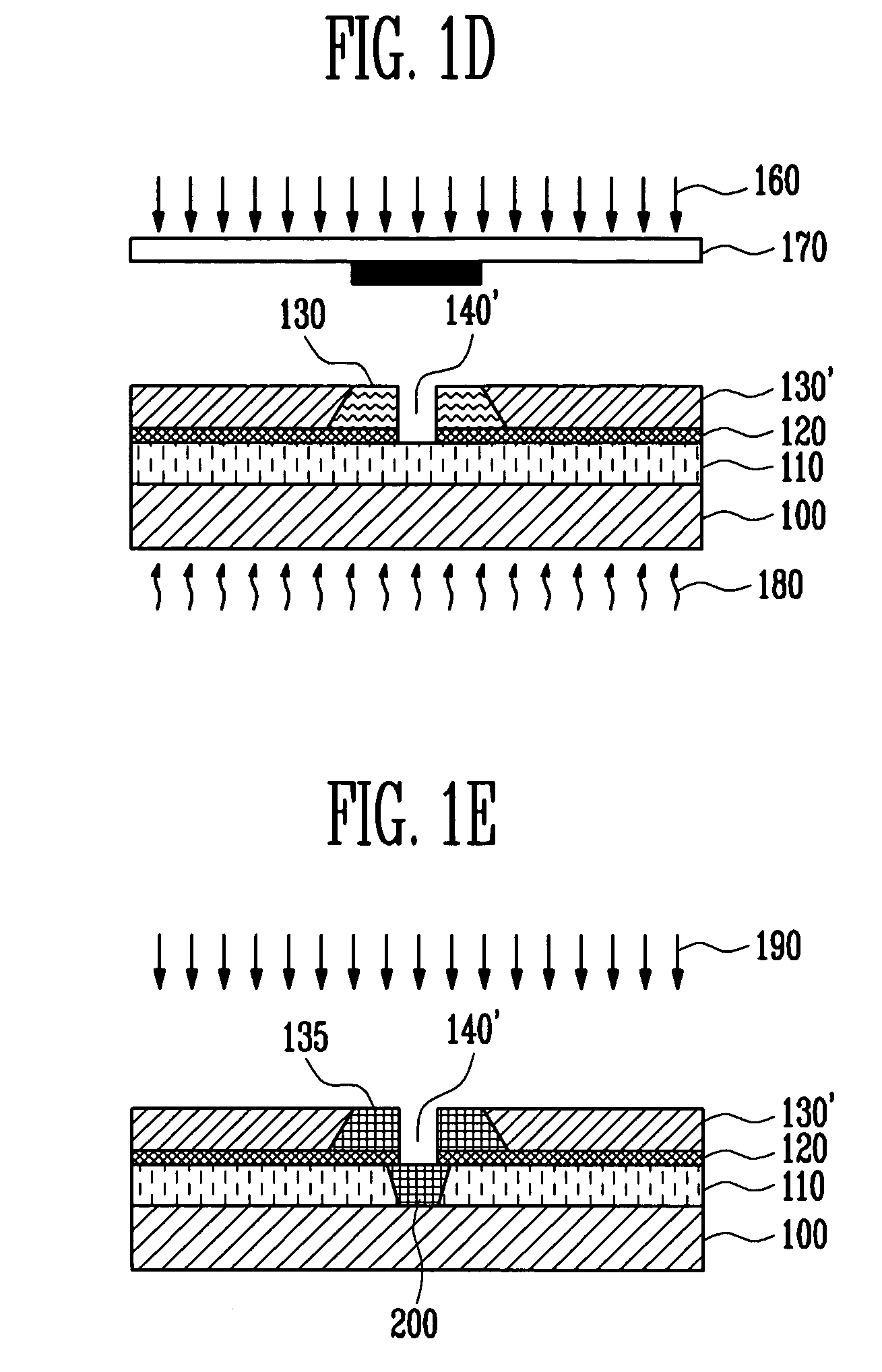
[0017]FIGS. 1A to 1H are cross-sectional views illustrating a method of fabricating a T-type gate in accordance with an embodiment of the present invention.

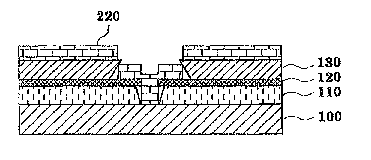
[0018]Referring to FIG. 1A, a lower photoresist layer 110 (for example, PFi-38A), which is sensitive to UV light, is formed to a predetermined thickness (for example, about 400 nm) on a compound wafer substrate 100, a blocking layer 120 (for example, made of Al or Ti) having a predetermined thickness (for example, about 20 nm) is deposited on the lower photoresist ...


PUM


Abstract

Provided is a method of fabricating a T-type gate including the steps of: forming a first photoresist layer, a blocking layer and a second photoresist layer to a predetermined thickness on a substrate, respectively; forming a body pattern of a T-type gate on the second photoresist layer and the blocking layer; exposing a predetermined portion of the second photoresist layer to form a head pattern of the T-type gate, and performing a heat treatment process to generate cross linking at a predetermined region of the second photoresist layer except for the head pattern of the T-type gate; performing an exposure process on an entire surface of the resultant structure, and then removing the exposed portion; and forming a metal layer of a predetermined thickness on an entire surface of the resultant structure, and then removing the first photoresist layer, the blocking layer, the predetermined region of the second photoresist layer in which the cross linking are generated, and the metal layer, whereby it is possible to readily perform a compound semiconductor device manufacturing process, and to reduce manufacturing cost by means of the increase of manufacturing yield and the simplification of manufacturing processes.

Description

CROSS-REFERENCE TO RELATED APPLICATION[0001]This application claims priority to and the benefit of Korean Patent Application No. 2004-81397, filed Oct. 12, 2004, the disclosure of which is incorporated herein by reference in its entirety.BACKGROUND[0002]1. Field of the Invention[0003]The present invention relates to a method of fabricating a T-type gate and, more particularly, to a method of fabricating a T-type gate capable of facilitating a compound semiconductor device manufacturing process, enhancing the yield, and reducing the manufacturing cost by forming two kinds of patterns from one kind of photoresist layer using electron beam and photolithography technologies and by interposing a blocking layer between upper and lower photoresist layers for reversing the patterns.[0004]2. Discussion of Related Art[0005]In general, in methods of fabricating a compound semiconductor device such as a metal semiconductor field effect transistor (MESFET), a high electron mobility transistor (H...

Claims


Application Information

Patent Timeline
Patent Type & Authority Patents(United States)
IPC IPC(8): H01L21/338
CPCH01L21/28587H01L21/18
Inventor PARK, JONG MOONPARK, KUN SIKYOO, SEONG WOOKYOON, YONG SUNKIM, SANG GIBAE, YOON KYULIM, BYUNG WONKOO, JIN GUNKIM, BO WOO
Owner ELECTRONICS & TELECOMM RES INST
Why Eureka
Try Eureka