
Apparatus and methods for cooling semiconductor integrated circuit chip packages

a technology of integrated circuit chips and cooling modules, which is applied in semiconductor devices, lighting and heating apparatus, and semiconductor/solid-state device details, etc. it can solve the problems of increasing power density, adversely affecting integrated circuit components, and increasing the problem of effective heat removal, so as to increase the structural integrity of the electronic assembly and reduce mechanical stresses

Active Publication Date: 2006-05-18
GLOBALFOUNDRIES US INC
View PDF10 Cites 47 Cited by
  • Summary
  • Abstract
  • Description
  • Claims
  • Application Information

AI Technical Summary

Benefits of technology

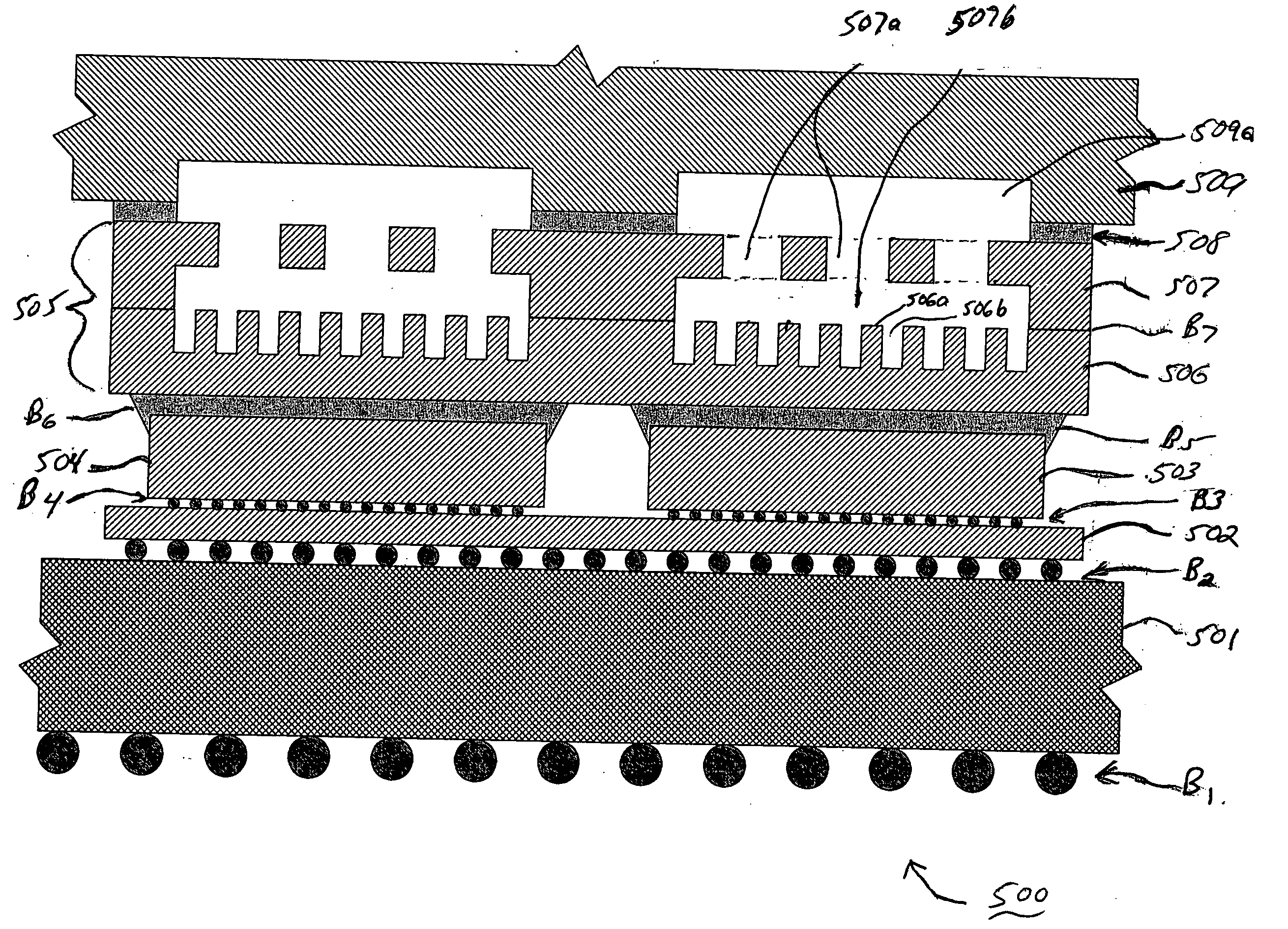
[0009] In another exemplary embodiment of the invention, an electronic module comprises a first level carrier substrate and an intermediate carrier substrate bonded to the first level carrier substrate, wherein the intermediate carrier substrate comprises a plurality of IC chips flip-chip bonded thereto. A cooling device, such as a microchannel cooler, is thermally bonded to the non-active surfaces of each IC chip mounted on the intermediate carrier substrate using rigid bonding material. The cooling device is formed of a material which is thermal expansion matched to the material from which the intermediate substrate carrier is formed to reduce mechanical stresses caused by differences in thermal expansion. The microchannel cooling device provides cooling for the chips and additionally increases the structural integrity of the electronic assembly by rigidly bonding the microchannel cooler to the back surfaces of IC chips mounted on the intermediate carrier. Moreover, microchannel cooler is light weight and the bonding material can be compatible with a C4 reflow, such that the microchannel cooler could be assembled to the intermediate carrier package with the IC chips before bonding the intermediate carrier package to the first level package.

Problems solved by technology

Effective heat removal becomes increasingly problematic as chip geometries are scaled down and operating speeds are increased, which results in increased power density.
Moreover, as chip packages or electronic modules become more compact with multiple IC chips densely packed together, the increased heat density generated by operation of the chips in such close proximity can adversely affect integrated circuit components and cause physical damage to the package structure due to differences in thermal expansion of the package components.
As reported in the literature, a practical silicon carrier thickness is primarily limited by the ultimate aspect ratio of the through vias.
In general, aspect ratio values much higher than about 10:1 are considered to be difficult to manufacture and make highly reliable.
Some of the practical difficulties which occur with a large area and thin silicon carrier include increased risk of fracturing the silicon carrier during processing, bonding or assembly, as well as providing an effective means for cooling the chips mounted on the silicon carrier.
It is difficult to use a conventional cooling means such as a thermal paste layer and a heat sink attached to the back surface of the chips since the force used to hold the heat sink in place and the large force used during assembly to insure a thin and uniform thermal paste layer could crack the silicon carrier.

Method used


Image

  • Apparatus and methods for cooling semiconductor integrated circuit chip packages
  • Apparatus and methods for cooling semiconductor integrated circuit chip packages
  • Apparatus and methods for cooling semiconductor integrated circuit chip packages

Examples


Embodiment Construction

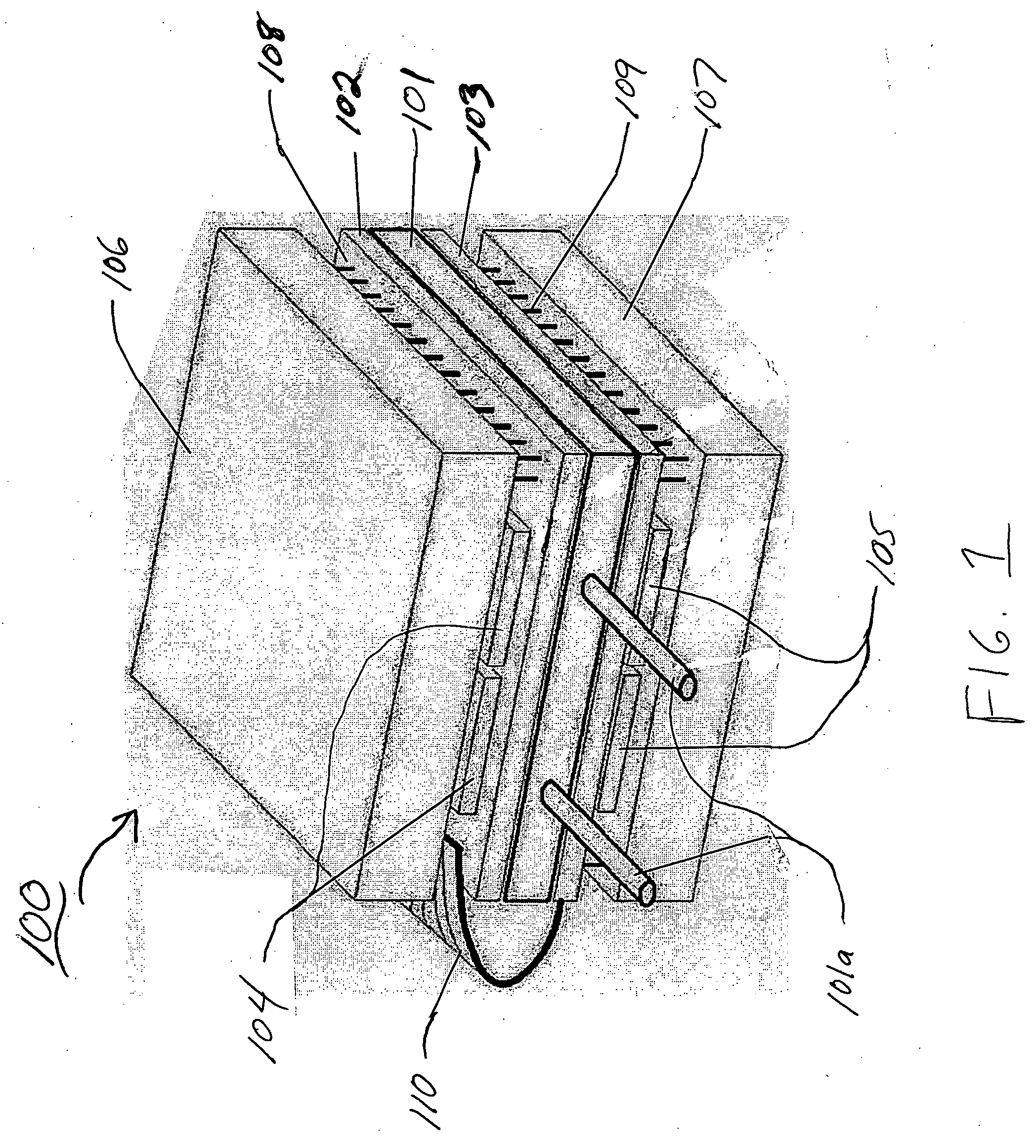
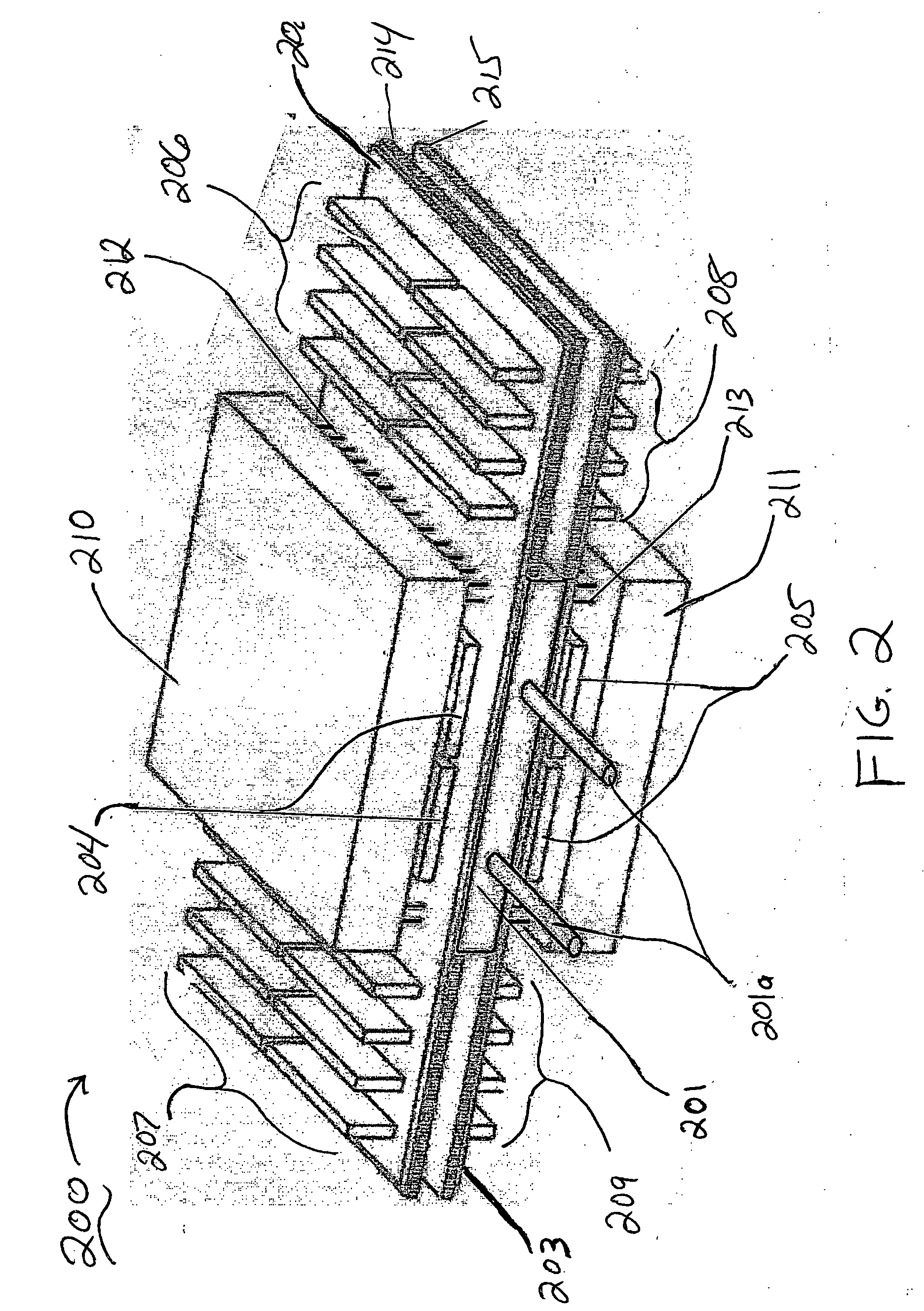
[0018]FIG. 1 is a schematic perspective view of an electronic module according to an exemplary embodiment of the invention. FIG. 1 schematically illustrates an exemplary embodiment of an electronic module (100) comprising an integrated cooling module (101) (e.g., microchannel cooler) with high-performance IC chips (102) and (103) bonded directly to the cooling module (101). The cooling device (101) comprises a microchannel cooling device having a plurality of coolant inlet / outlets (101a) to enable coolant to flow in and out of the cooling device (101). In one exemplary embodiment, the electronic module (100) comprises a computer “system on a package” in a stacked chip structure, wherein the IC chips (102) and (103) are processor chips (e.g., CPUs, microprocessors, etc.). The back (non-active) surfaces of the IC processor chips (102) and (103) are thermally coupled to opposite surfaces of the cooling device (101). Furthermore, an array of IC memory chips (104) and (105) are flip-chip...


PUM


Abstract

Apparatus and methods are provided for integrating microchannel cooling modules within high-density electronic modules (e.g., chip packages, system-on-a-package modules, etc.,) comprising multiple high-performance IC chips. Electronic modules are designed such that high-performance (high power) IC chips are disposed in close proximity to the integrated cooling module (or cooling plate) for effective heat extraction. Moreover, electronic modules which comprise large surface area silicon carriers with multiple chips face mounted thereon are designed such that integrated silicon cooling modules are rigidly bonded to the back surfaces of such chips to increase the structural integrity of the silicon carriers.

Description

TECHNICAL FIELD OF THE INVENTION [0001] The present invention relates generally to apparatus and methods for packaging semiconductor IC (integrated circuit) chips with integrated cooling modules. More specifically, the present invention relates to apparatus and methods for integrating microchannel cooling modules within high-density chip packages and system-on-a-package modules comprising multiple high-performance IC chips. BACKGROUND [0002] In the design and manufacture of semiconductor IC chip packages and modules (e.g., SCM (single chip modules), MCMs (multi-chip modules), etc.), it is imperative to implement mechanisms that can effectively remove heat generated by IC chips, such as microprocessors or other high-performance chips, to ensure continued reliable operation of the IC chips. Effective heat removal becomes increasingly problematic as chip geometries are scaled down and operating speeds are increased, which results in increased power density. Moreover, as chip packages o...

Claims


Application Information

Patent Timeline
Patent Type & Authority Applications(United States)
IPC IPC(8): H01L23/34
CPCH01L23/473H01L25/0657H01L2224/73253H01L2225/06517H01L2225/06589H01L2924/15311H01L2224/16225H01L2224/32245H01L2924/01019H01L2924/00014H01L2924/00011H01L2224/0401
Inventor ANDRY, PAUL S.COLGAN, EVAN G.MOK, LAWRENCE S.PATEL, CHIRAG S.SEEGER, DAVID E.
Owner GLOBALFOUNDRIES US INC
Learn More