Driver circuit and display device

a driver circuit and display device technology, applied in the field of driver circuits and display devices, can solve the problems of increasing chip size, consuming a lot of power, and causing burn-in of display images, so as to reduce the total power consumption of the driver circuit

Inactive Publication Date: 2006-05-18
RENESAS ELECTRONICS CORP
View PDF3 Cites 34 Cited by
  • Summary
  • Abstract
  • Description
  • Claims
  • Application Information

AI Technical Summary

Benefits of technology

[0015] The present invention provides a driver circuit for inversion-driving a liquid crystal display panel, including: a positive-polarity line transmitting a positive display signal relative to a reference voltage; a negative-polarity line transmitting a negative display signal relative to the reference voltage; a switching part switching the positive-polarity line and the negative-polarity line from each other to be connected with a source line; and a charge recovery circuit part connected with the positive-polarity line through a first switching element and connected with the negative-polarity line through a second switching element. According to the driver circuit of the present invention, the total power consumption of the driver circuit can be reduced.

Problems solved by technology

When the liquid crystal display device is driven with DC voltage, a problem arises in that the display image causes burn-in due to, for example, degradation of liquid crystal components, and contamination with impurities mixed in the liquid crystal display panel.
In the case of using this AC driving system, the common electrode is alternately applied with the positive voltage and the negative voltage, which consumes much power.
This leads to a problem of an increased chip size.
As a result, the power consumption is increased.

Method used


Image

  • Driver circuit and display device
  • Driver circuit and display device
  • Driver circuit and display device

Examples


first embodiment

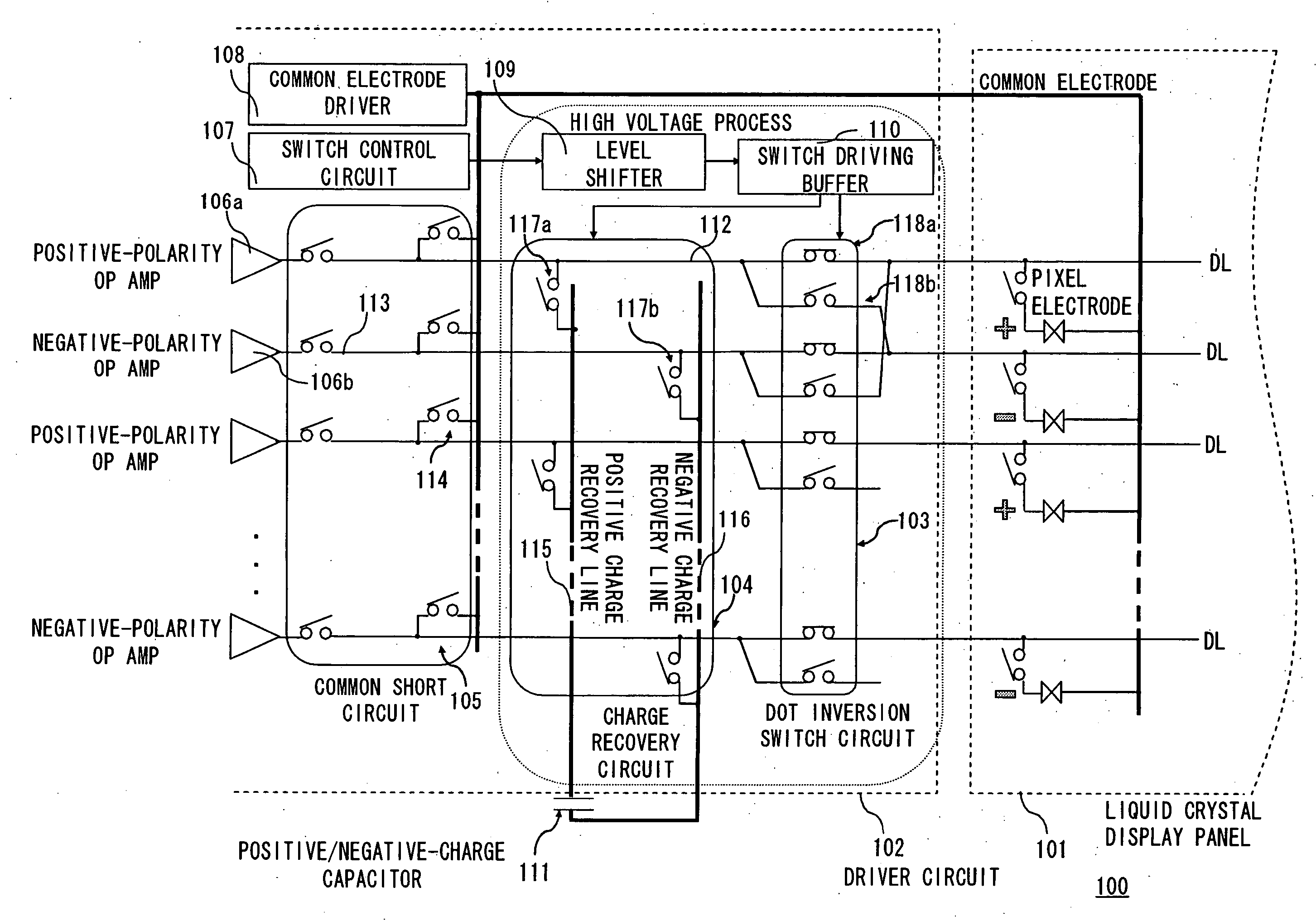
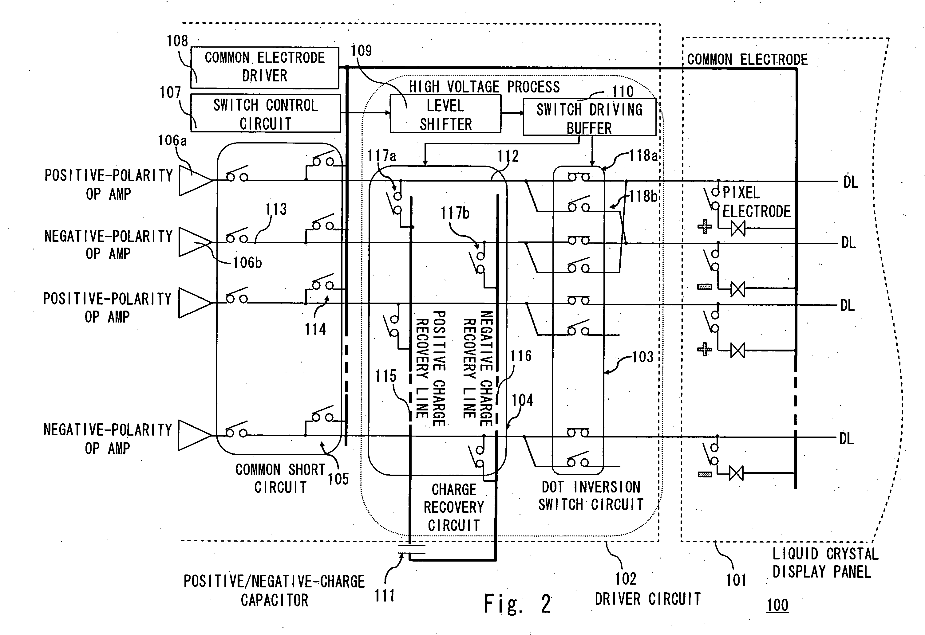
[0036]FIG. 2 is a circuit diagram showing the driver circuit 102 according to a first embodiment. The driver circuit 102 includes a dot inversion switch circuit 103, a charge recovery circuit 104, a common short circuit 105, an operational amplifier 106, a switch control circuit 107, a common electrode driver 108, a level shifter 109, and a switch driving buffer 110. For illustrative purposes, pixels in the liquid crystal display panel 101 are shown. In FIG. 2, the horizontal direction of the liquid crystal display panel 101 is defined as a direction in which the source line DL extends, and the vertical direction is defined as a direction in which the gate line GL extends.

[0037] In this embodiment, the operational amplifier 106, the common short circuit 105, the charge recovery circuit 104, and the dot inversion switch circuit 103 are arranged in the stated order. Arranged on the output side of the dot inversion switch circuit 103 is the liquid crystal display panel 101.

[0038] As ...

second embodiment

[0063]FIG. 5 is a circuit diagram showing the driver circuit 102 according to a second embodiment of the present invention. The driver circuit 102 includes the dot inversion switch circuit 103, the charge recovery circuit 119, the common short circuit 105, the operational amplifier 106, the switch control circuit 107, the common electrode driver 108, the level shifter 109, and the switch driving buffer 110. In FIG. 5, the same components as the first embodiment are denoted by like reference numerals and their detailed description is omitted herein. The driver circuit 102 according to the second embodiment differs from that of the first embodiment in that the positive-charge capacitor 120 and negative-charge capacitor 121 are separately provided in the charge recovery circuit 119.

[0064] In this embodiment, the operational amplifier 106, the common short circuit 105, the charge recovery circuit 104, and the dot inversion switch circuit 103 are arranged in the stated order. The liquid...

third embodiment

[0079]FIG. 9 is a circuit diagram showing the driver circuit 102 according to a third embodiment of the present invention. The driver circuit 102 includes the dot inversion switch circuit 103, the charge recovery circuit 119, the operational amplifier 106, the switch control circuit 107, the common electrode driver 108, the level shifter 109, the switch driving buffer 110, and a D / A converter 124. In FIG. 9, the same components as the first embodiment are denoted by like reference numerals, and their description is omitted here. The driver circuit 102 of the third embodiment is different from the second embodiment in that the common short circuit 105 is omitted, and the D / A converter 124 is provided on the input terminal side of the operational amplifier 106.

[0080] The input side of the D / A converter 124 is connected with the gradation data transmission line and a line transmitting common electrode data output from the common electrode driver 108. The D / A converter 124 converts dig...


PUM


Abstract

To provide a driver circuit that enables reduction in the number of elements formed through a high-voltage process and in chip size. An embodiment of the present invention relates to a driver circuit for inversion-driving a liquid crystal display panel, including: a positive-polarity line transmitting a positive display signal relative to a common electrode signal; a negative-polarity line transmitting a negative display signal relative to the common electrode signal; a dot inversion switch circuit switching the positive-polarity line and the negative-polarity line from each other to be connected with a source line; a charge recovery circuit connected with the positive-polarity line through a positive charge recovery switch and connected with the negative-polarity line through a negative charge recovery switch; and a common short circuit connecting the positive-polarity line and the negative-polarity line with a common electrode.

Description

BACKGROUND OF THE INVENTION [0001] 1. Field of the Invention [0002] The present invention relates to a driver circuit and a display device. [0003] 2. Description of Related Art [0004] Along with recent developments in advanced image / information-oriented society, and popularization of multimedia systems, flat display panels such as a liquid crystal display device have gained increasing importance. The liquid crystal display devices have been widely used as a display device of a portable terminal device etc. because of its low power consumption, slimness, light weight, and other such advantages. [0005] In general, the liquid crystal display device includes a liquid crystal display panel for displaying an image, and a driver circuit for driving the liquid crystal display panel. The liquid crystal display panel includes: a TFT array substrate on which pixel electrodes are arranged in matrix, and switching elements such as TFTs (thin film transistors) are connected with the pixel electro...

Claims


Application Information

Patent Timeline
Patent Type & Authority Applications(United States)
IPC IPC(8): G09G3/36
CPCG09G3/3614G09G3/3688G09G2310/0251G09G2310/0289G09G2310/0297G09G2330/021G09G2330/023
Inventor MIURA, MAKOTO
Owner RENESAS ELECTRONICS CORP
Why Eureka
Try Eureka