

Memory element and memory device
- Summary
- Abstract
- Description
- Claims
- Application Information
AI Technical Summary
Benefits of technology
Problems solved by technology
Method used
Image

Examples
example 1 and practice example 2
(Practice Example 1 and Practice Example 2)
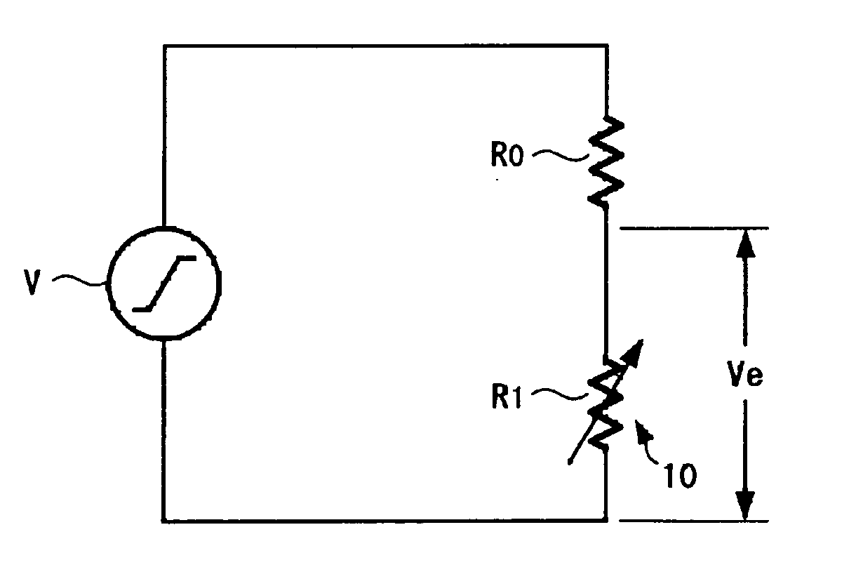
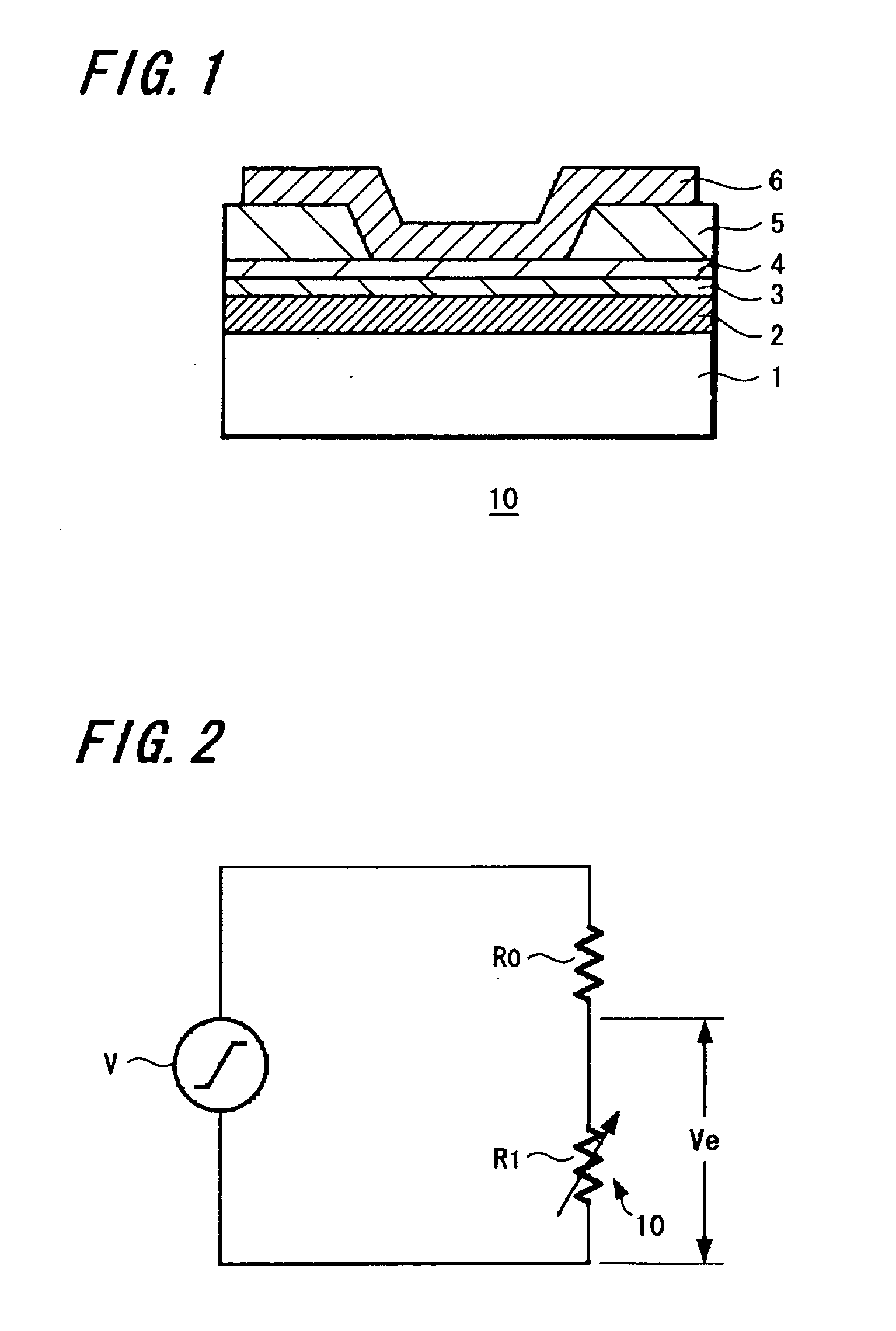
[0146] Next, the memory element 10 shown in FIG. 1 was produced to make a sample of the memory element 10 of a practice example 1, in which a CuTeGeGd film having a film thickness of 20 nm was formed as the ion source layer 3, a Gd oxide film having a film thickness of 3 nm was formed as the memory layer 4, a TiW film was formed as the upper electrode 6, and those other than that were made similar to the experiment 1 (sample of the comparison example).
[0147] Further, the memory element 10 shown in FIG. 1 was produced to make a sample of the memory element 10 of an practice example 2, in which the film thickness of the Gd oxide film of the memory layer 4 was made into 1.4 nm, and the other structure than that was made similar to the sample of the practice example 1.
[0148] Similarly to the experiment 1 except for a change in the range of the applied voltage, an electric current was measured by sweeping a voltage repeatedly with respect to e...
example 3
(Practice Example 3)
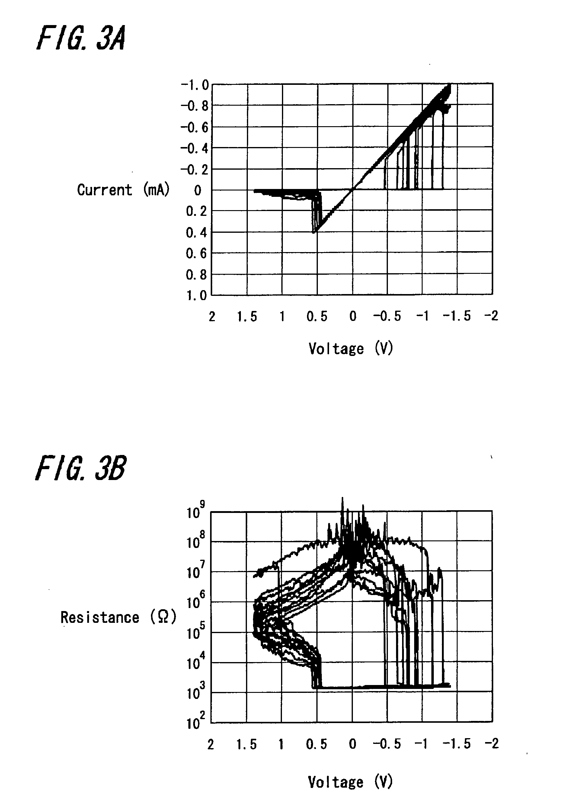
[0185] Next, a memory element was produced by changing the material of the memory layer 4, whose electrical resistivity was low, and a characteristic was examined similarly.
[0186] The memory element 10 was produced to make a sample of the memory element 10 of a practice example 3, in which a GdW oxide film having a film thickness of 3 nm was formed as the memory layer 4, and other than that was made similarly to the sample of the experiment 2.
[0187] The resistivity of the memory layer 4 of the memory element in the practice example 3 was 1.1×10² (Ωcm).
[0188] An electric current was measured by repeatedly sweeping a voltage for the sample of the memory element 10 of this practice example 3, while the others were similar to the experiment 1 and experiment 2. Further, a resistance value was calculated from each value of the voltage and electric current.
[0189]FIG. 6A shows a resistance-voltage characteristic in a case where a range of an applied voltage is set fr...
PUM
 Abstract
Description
Claims
Application Information