Semiconductor memory system and method for the transfer of write and read data signals in a semiconductor memory system

a memory system and semiconductor technology, applied in the field of semiconductor memory systems, can solve the problems of excessively increasing the cost of such a system, unable to detect and correct errors, and unable to use the transfer of separate dqs signals for synchronization,

Active Publication Date: 2006-05-18
POLARIS INNOVATIONS
View PDF3 Cites 0 Cited by
  • Summary
  • Abstract
  • Description
  • Claims
  • Application Information

AI Technical Summary

Benefits of technology

[0005] Accordingly, the present invention aims at facilitating a semiconductor memory system of the aforementioned type and a method for the transfer of write and read data signals among the interface circuits in such a semiconductor memory system, wherein the detection and/or correction of erro

Problems solved by technology

Typically, however, conventional DIMM memory modules for desktop personal computers do not have the capability to detect and correct errors.
An additional further module for the detection and/or correction of errors that is not used for the storing of data would excessively increase the cost of such a system.
Since it might collide with read data or write data, the sync

Method used


Image

  • Semiconductor memory system and method for the transfer of write and read data signals in a semiconductor memory system
  • Semiconductor memory system and method for the transfer of write and read data signals in a semiconductor memory system
  • Semiconductor memory system and method for the transfer of write and read data signals in a semiconductor memory system

Examples


Embodiment Construction

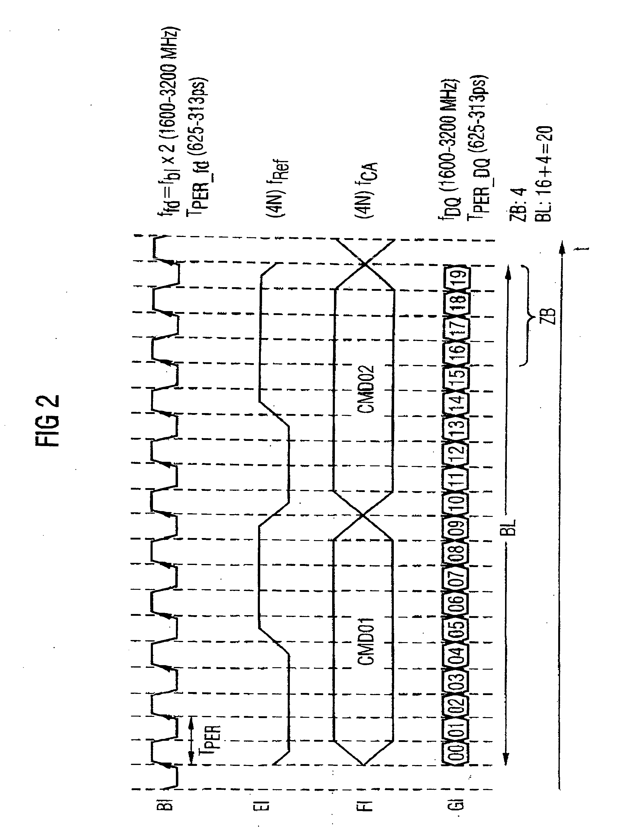
[0020] The following illustration of a preferred embodiment of the invention by means of FIGS. 1 and 2 will be preceded by a description of the prior art signal-time diagram of FIG. 3 illustrating a conventional method for the transfer of write and read data signals. According to this transfer method and on the basis of the fundamental clock of the frequency fb1 shown in the first line A, for example within a frequency range fb1=800-1600 MHz corresponding to a period length PPR—b1 of 1250-625 ps, and a fundamental clock of the frequency 1.5×fb1 that is shown in the second line B and is immediately derived from the fundamental clock according to line A, for example within a frequency range of 1333-2400 MHz corresponding to a period length of 750-416 ps, either a reference clock fref with a period length Tper—ref that is shown in the third line C is generated according to a “2N” rule which means that a CA unit interval is twice the period length of the fundamental clock according to t...


PUM


Abstract

A semiconductor memory system for the transfer of write and read data signals among interface circuits includes at least one memory device, a memory controller unit and, optionally, a register unit of a semiconductor memory system, wherein the data signals are each transferred in signal bursts of a specific burst length. The system is characterized in that a number of additional bits extending the burst length are transferred together with at least every nth signal burst.

Description

FIELD OF THE INVENTION [0001] The present invention relates to a semiconductor memory system. More particularly, the present invention relates to a semiconductor memory system with at least one memory device, a memory controller unit and, an optional register unit. Each of these components comprises an interface circuit and a method for the transfer of write and read data signals among the interface circuits, the data signals each being transferred in signal bursts of a specific burst length. DESCRIPTION OF THE RELATED ART [0002] At present, a separate ECC-module that can detect and possibly correct a channel error or a data error resulting from a DRAM error is provided for the detection or correction of errors in memory modules that are equipped with high-speed semiconductor memory devices. Typically, however, conventional DIMM memory modules for desktop personal computers do not have the capability to detect and correct errors. An additional further module for the detection and / or...

Claims


Application Information

Patent Timeline
IPC IPC(8): G11C7/00
CPCG11C5/04G11C7/1018G11C7/1045
Inventor RUCKERBAUER, HERMANNSAVIGNAC, DOMINIQUESICHERT, CHRISTIANGREGORIUS, PETERWALLNER, PAUL
Owner POLARIS INNOVATIONS
Why Eureka
Try Eureka