Signal transmission structure and circuit substrate thereof

Active Publication Date: 2006-05-25
VIA TECH INC
View PDF15 Cites 13 Cited by
  • Summary
  • Abstract
  • Description
  • Claims
  • Application Information

AI Technical Summary

Benefits of technology

[0013] Accordingly, at least one objective of the present invention is to provide a signal t

Problems solved by technology

However, this method requires larger layout area and hence cannot be applied to a limited or high-density area of circuit layout.
As a result, signal transmission quality will be affected.
For transmission of a single signal or a differential signal, the higher the operating frequency, corresponding to a same operating frequency, the greater the return loss is when the signal passes the through hole 132, so that impedance mis

Method used


Image

  • Signal transmission structure and circuit substrate thereof
  • Signal transmission structure and circuit substrate thereof
  • Signal transmission structure and circuit substrate thereof

Examples


Example

[0025] Reference will now be made in detail to the present preferred embodiments of the invention, examples of which are illustrated in the accompanying drawings. Wherever possible, the same reference numbers are used in the drawings and the description to refer to the same or like parts.

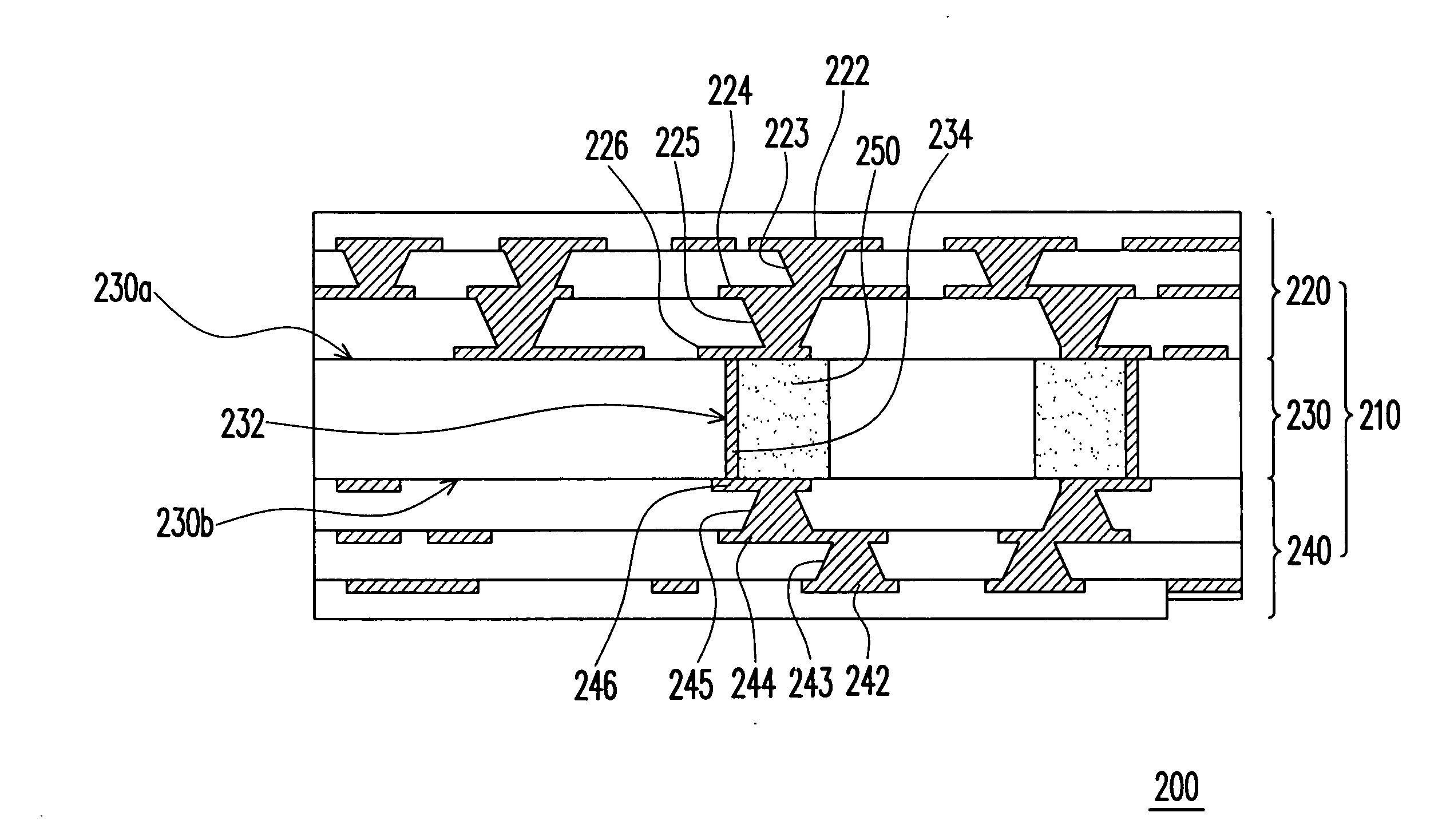
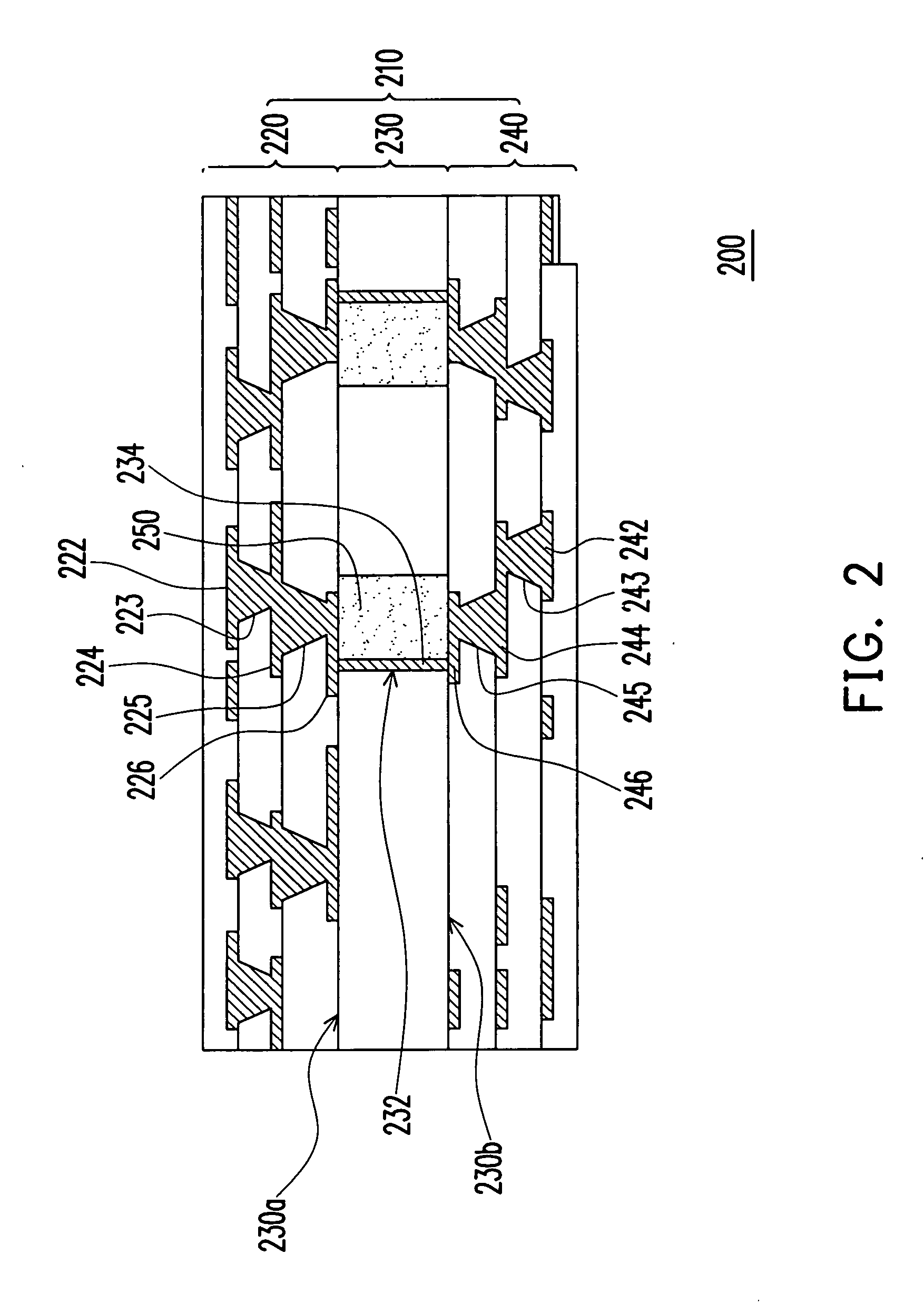
[0026]FIG. 2 is a schematic cross-sectional view of a circuit substrate according to one preferred embodiment of the present invention. A circuit substrate 200 having altogether six layers of patterned circuit layers and dielectric layer is used as an example in FIG. 2. The circuit substrate 200 has a multi-layer circuit structure 210 comprising a top circuit structure 220, a core layer 230 and a bottom circuit structure 240. The top circuit structure 220 comprises a plurality of patterned circuit layers and at least a dielectric layer alternately laid over each other above the core layer 230. The via lands 224, 226 in each patterned circuit layer are electrically connected to each other through a ...


PUM


Abstract

A signal transmission structure is provided. The structure mainly comprises at least a conductive via, at least a via land and a conductive wall. One end of the conductive via is connected to the via land. The conductive wall covers only a portion of the inner wall of a through hole in the core layer of a circuit substrate. The conductive wall has a semi-circular or a C-shaped structure. Therefore, when a signal passes the conductive via and the via land of the circuit substrate through the conductive wall in the interior of the via, because of a more continuous impedance between the via land and the conductive wall, signal reflection due to impedance mismatch along the signal transmission pathway can be reduced to enhance signal transmission quality.

Description

CROSS-REFERENCE TO RELATED APPLICATION [0001] This application claims the priority benefit of Taiwan application serial no. 93136103, filed on Nov. 24, 2004. BACKGROUND OF THE INVENTION [0002] 1. Field of the Invention [0003] The present invention relates to a signal transmission structure. More particularly, the present invention relates to a signal transmission structure and circuit substrate thereof capable of reducing insertion loss during signal transmission. [0004] 2. Description of the Related Art [0005] A conventional circuit substrate comprises a multiple patterned circuit layers and a plurality of dielectric layers alternately laminated on top of each other. The patterned circuit layers are formed, for example, by patterning copper foils in photolithographic and etching processes. The dielectric layers are disposed between neighboring patterned circuit layers to isolate the patterned circuit layers. In addition, the laminated circuit layers are electrically connected to ea...

Claims


Application Information

Patent Timeline
IPC IPC(8): H05K1/03
CPCH05K1/0216H05K1/115H05K3/4602H05K2201/09536H05K2201/0959H05K2201/09645
Inventor HSU, JIMMYHSU, CHI-HSING
Owner VIA TECH INC
Why Eureka
Try Eureka