

Nitride semiconductor device and method of manufacturing the same
a technology of semiconductor devices and semiconductors, applied in semiconductor/solid-state device manufacturing, semiconductor devices, electrical equipment, etc., can solve problems such as difficulty in manufacturing laser diodes, and achieve the effects of stable operation and output, reduced operation voltage for laser diodes, and reduced variations in the properties of laser diodes due to heat produced during operation
- Summary
- Abstract
- Description
- Claims
- Application Information
AI Technical Summary
Benefits of technology
Problems solved by technology
Method used
Image

Examples
first embodiment
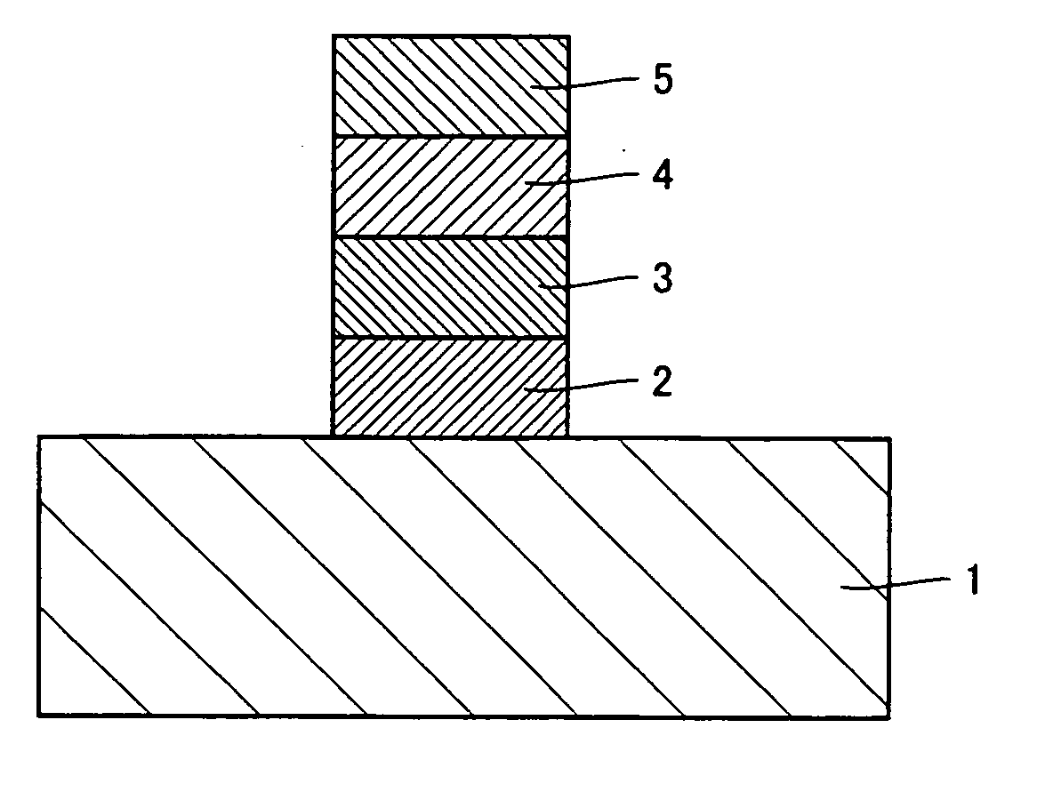
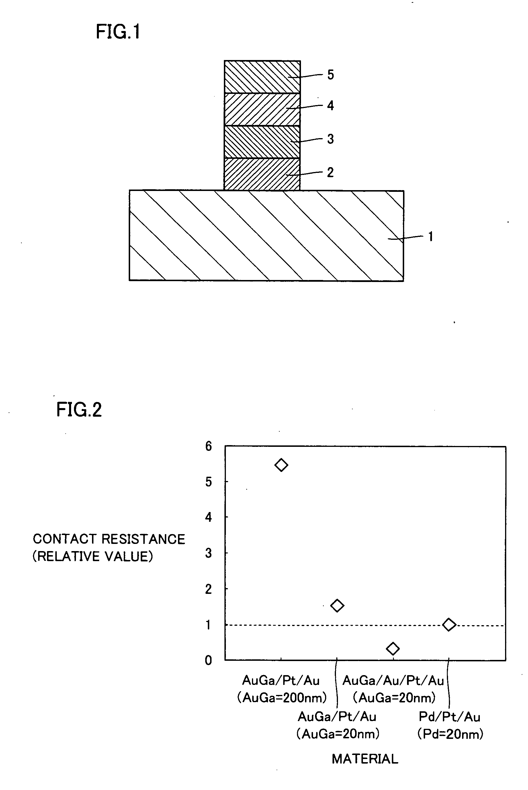
[0023] A nitride semiconductor device according to a first embodiment of the present invention is described using FIG. 1. As shown in FIG. 1, a P-type electrode is provided on a P-type contact layer 1 in the semiconductor device of this embodiment. The P-type electrode is formed with an AuGa film 2, an Au film 3, a Pt film 4, and an Au film 5. AuGa film 2 is provided on P-type contact layer 1. Au film 3 is provided on AuGa film 2. Pt film 4 is provided on Au film 3. Au film 5 is provided on Pt film 4. In the nitride semiconductor device described above, a P-type AlxGa1-xN (0≦x≦1) is used as P-type contact layer 1 which is a nitride semiconductor.
[0024] Next, a relationship between a material of a P-type electrode and a relative value of a contact resistance is described using FIG. 2. The relative value of the contact resistance of the P-type electrode indicated in FIG. 2 is a ratio to a contact resistance of a conventional P-type electrode using a Pd film. In this specification, “a...
second embodiment
[0037] A nitride semiconductor device of a second embodiment of the present invention is described using FIG. 10. In the nitride semiconductor device of this embodiment, a P-type electrode material is provided on a top surface of P-type contact layer 1. The P-type electrode is formed with an Au film 8, an AuGa film 9, Pt film 4, and Au film 5. Au film 8 is provided on P-type contact layer 1. AuGa film 9 is provided on Au film 8. Pt film 4 is provided on AuGa film 9. Au film 5 is provided on Pt film 4.
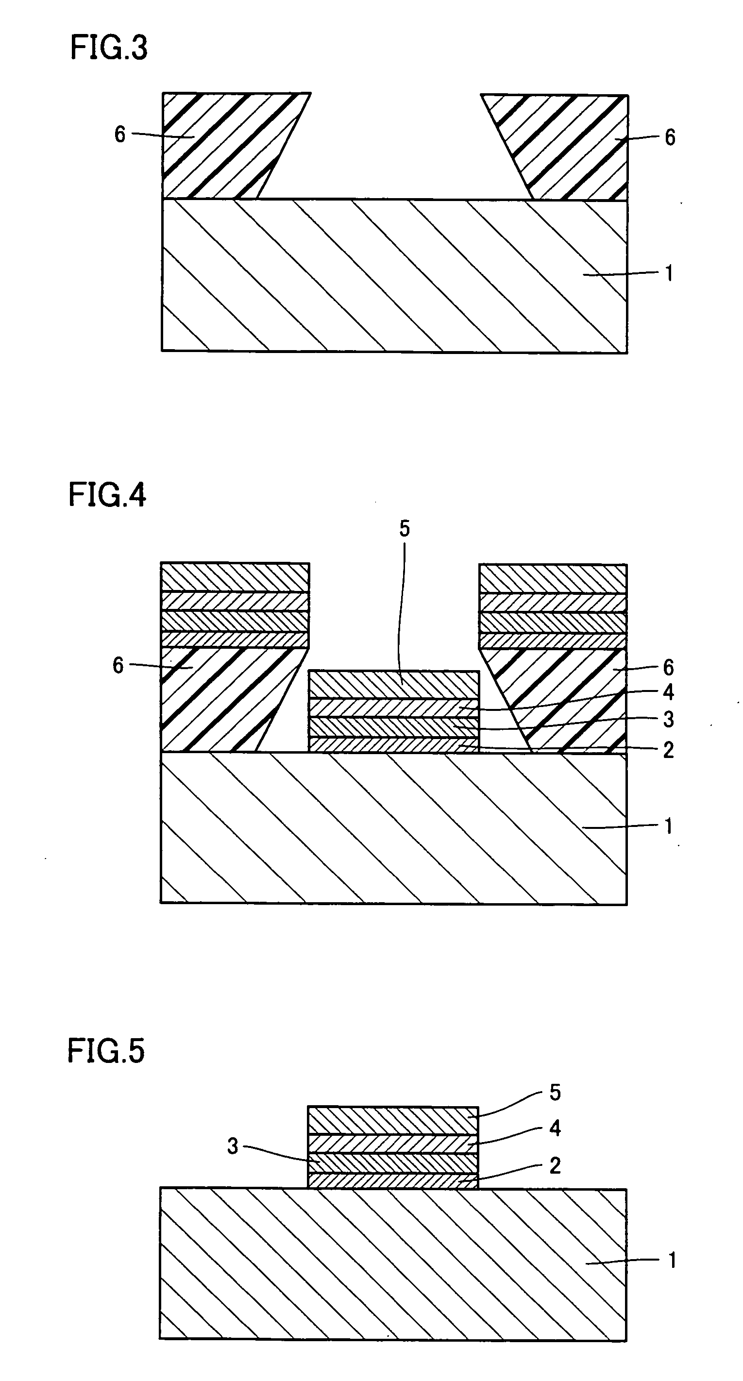
[0038] Next, a method of manufacturing the nitride semiconductor device having a structure as described above is described. The method of manufacturing is basically similar to that in the first embodiment described using FIGS. 3-5. The method of manufacturing the nitride semiconductor device of this embodiment, however, has an order of deposition of materials forming the P-type electrode different from that in the method of manufacturing the nitride semiconductor device of the first em...
PUM
| Property | Measurement | Unit |
|---|---|---|
| temperature | aaaaa | aaaaa |
| temperature | aaaaa | aaaaa |
| thickness | aaaaa | aaaaa |
Abstract
Description
Claims
Application Information