Distributed feedback semiconductor laser and method for manufacturing the same

a semiconductor laser and semiconductor technology, applied in semiconductor lasers, optical resonator shape and construction, laser details, etc., can solve the problems of difficult control of etching depth, large interior loss, and restricted single wave oscillation within 30%, so as to achieve easy manufacturing

Inactive Publication Date: 2006-05-25
SAMSUNG ELECTRONICS CO LTD
View PDF6 Cites 1 Cited by
  • Summary
  • Abstract
  • Description
  • Claims
  • Application Information

AI Technical Summary

Benefits of technology

[0012] Another aspect of the present invention relates a method for manufacturing a distributed feedback semiconductor lase...

Problems solved by technology

Generally, the DFB laser has a problem in that the diffraction gratings of a light emitting surface are arbitrarily cut off and the oscillation of the single wave is restricted to within 30%.
First, since the etched degree of the active layer greatly affects the difference of the gain, the etching depth must be accurately regulated.
However, since the thickness of each layer in MQW is un...

Method used


Image

  • Distributed feedback semiconductor laser and method for manufacturing the same
  • Distributed feedback semiconductor laser and method for manufacturing the same
  • Distributed feedback semiconductor laser and method for manufacturing the same

Examples


first embodiment

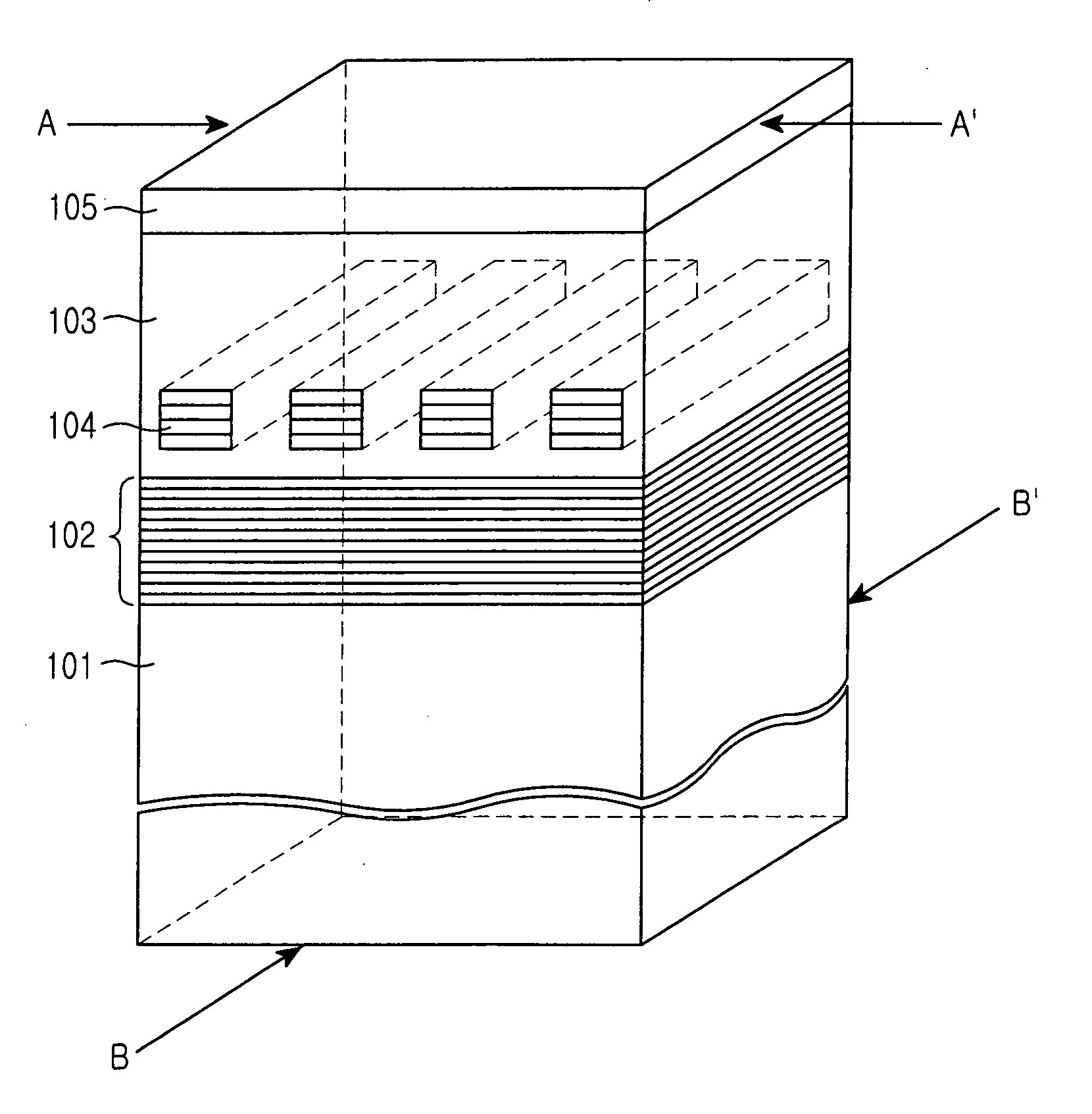
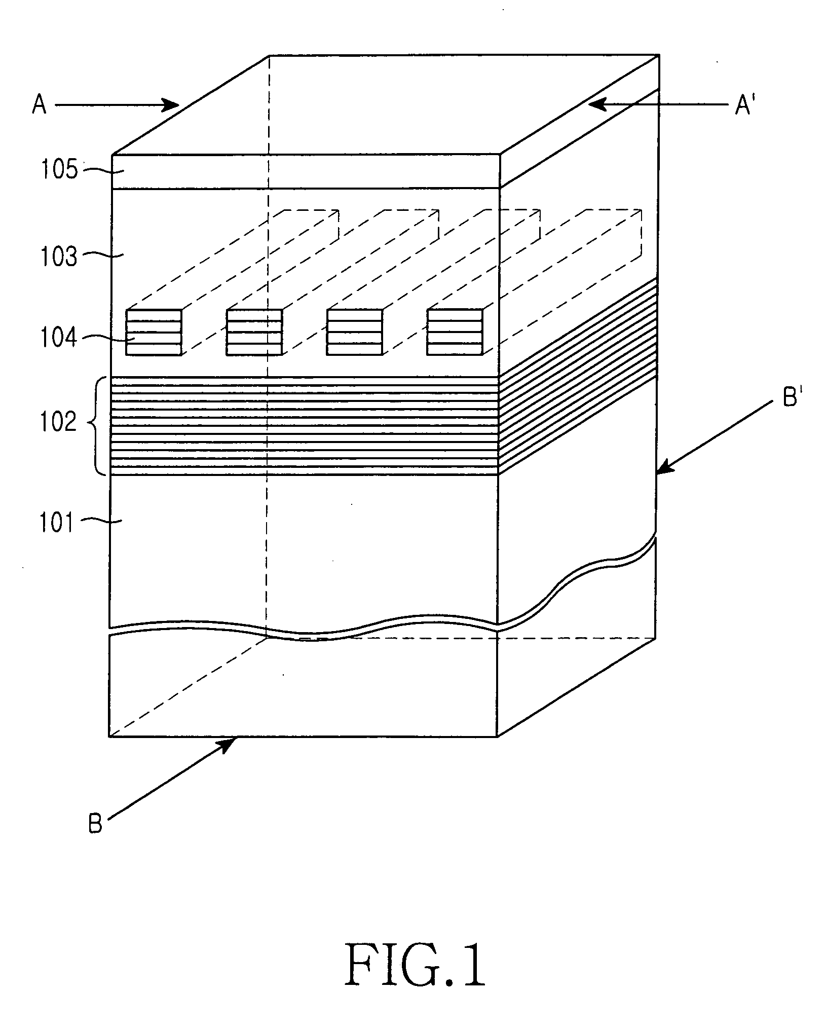
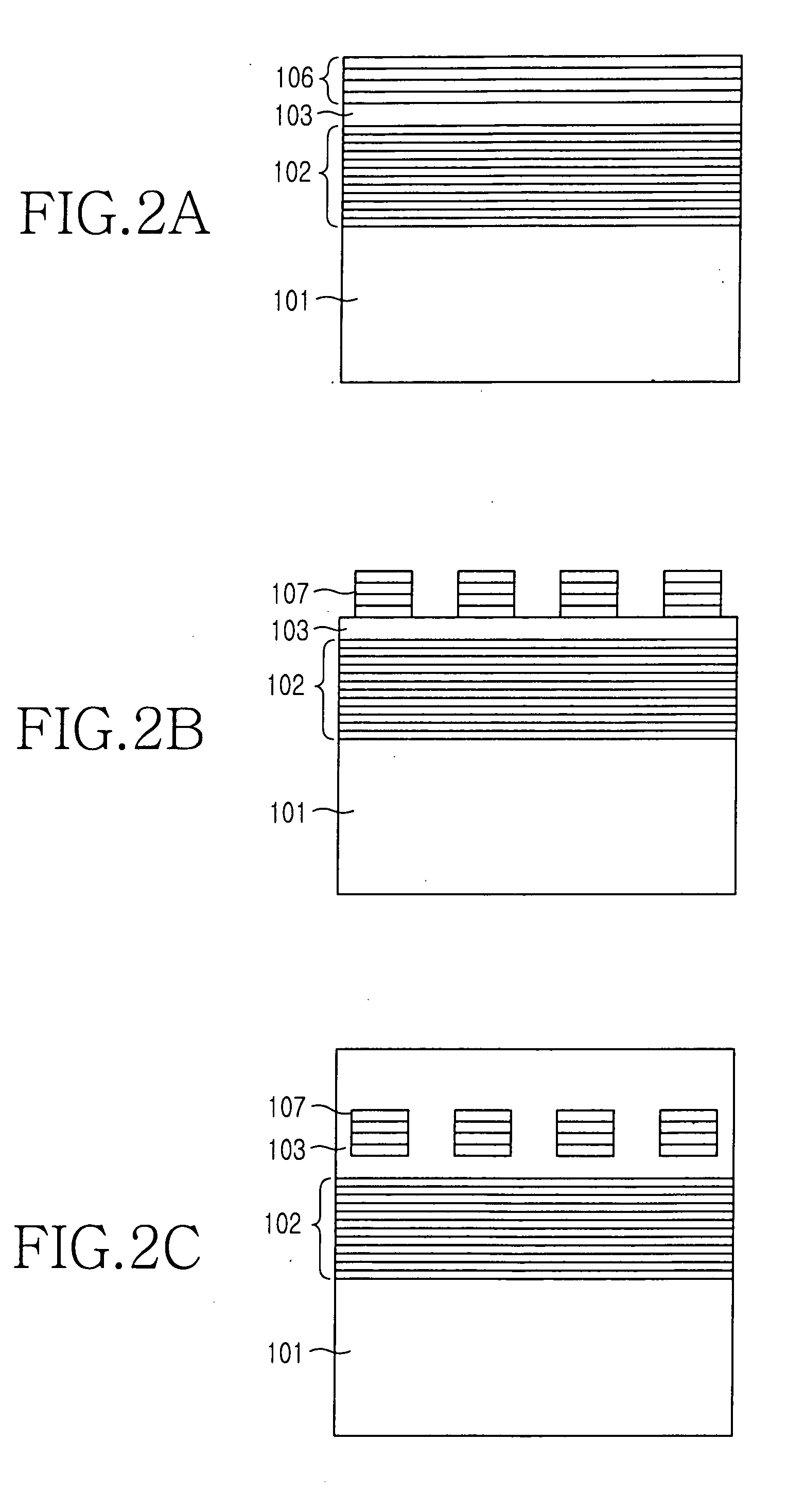
[0025]FIG. 1 is a perspective view for showing a distributed feedback semiconductor laser 100 according to the present invention.

[0026] The distributed feedback semiconductor laser 100 includes a substrate 101, an active layer 102 formed on the substrate 101 and a clad layer 103, which is formed on the active layer 102 and of a different conductive type from the substrate 101. The laser 100 also includes diffraction gratings 104 periodically formed in the clad layer 103 and separated from each other by a predetermined distance, a contact layer 105, which is formed on the upper portion of the clad layer 103 and of a different conductive type from the substrate 101.

[0027] The substrate 101 is an n-type compound semiconductor substrate. The active layer 102 of a MQW (multiple quantum well) structure in which several n-type compound semiconductor layers are stacked. The clad layer 103 of p-type is formed on the active layer 102. The above structure is not deviated greatly from the appl...

second embodiment

[0038]FIG. 3 is a perspective view for showing a distributed feedback semiconductor laser 200 according to the present invention.

[0039] The distributed feedback semiconductor laser 200 includes a substrate 201, a clad layer 202 which is formed on the substrate 201 and of the same conductive type as the substrate 201 and nonconductive diffraction gratings 203 periodically formed in the clad layer 202 and separated from each other by a predetermined distance. The laser 200 also includes an active layer 204 formed on the clad layer 202, a contact layer 206 which is formed on the upper portion of the clad layer 205 and of a different conductive type from the substrate 201. In the second embodiment, the nonconductive diffraction gratings 203 are formed below the active layer 204. By spatially differentiating the electron carrier (in the case of n-type substrate) injected from the substrate direction, the local difference of the gain coefficient is obtained. Since the structure and operat...

third embodiment

[0040]FIG. 4 is a perspective view for showing a distributed feedback semiconductor laser 300 according to the present invention.

[0041] The distributed feedback semiconductor laser 300 includes a substrate 301, a clad layer 302 which is formed on the substrate 301 and of the same conductive type as the substrate 301 and nonconductive diffraction gratings 303 periodically formed in the clad layer 302 and separated from each other by a predetermined distance The laser 300 also includes an active layer 304 formed on the clad layer 302, a clad layer 305 which is formed on the active layer 304 and of the different conductive type from the substrate 301, nonconductive upper diffraction gratings 303 periodically formed in the clad layer 305 and separated from each other by a predetermined distance, and a contact layer 306 which is formed on the clad layer 305 and of a different conductive type from the substrate 201. In the third embodiment, the nonconductive diffraction gratings 303 are f...


PUM


Abstract

A distributed feedback semiconductor laser oscillating in a single mode and a method for manufacturing the same is disclosed. The distributed feedback semiconductor laser includes an active layer; a clad layer formed adjacent to the active layer; and diffraction gratings periodically formed in the clad layer and separated from each other by a predetermined distance. The diffraction gratings are formed of a nonconductor so that a current injected into the active layer is partially blocked and distribution of gain coefficient is varied. The nonconductor is an oxidized semiconductor material.

Description

CLAIM OF PRIORITY [0001] This application claims priority to an application entitled “DISTRIBUTED FEEDBACK SEMICONDUCTOR LASER AND METHOD FOR MANUFACTURING THE SAME,” filed with the Korean Intellectual Property Office on Nov. 24, 2004 and assigned Ser. No. 2004-97126, the contents of which are incorporated herein by reference. BACKGROUND OF THE INVENTION [0002] 1. Field of the Invention [0003] The present invention relates to a distributed feedback semiconductor laser, and more particularly to a distributed feedback semiconductor laser oscillating in a single mode and a method of manufacturing the same. [0004] 2. Description of the Related Art [0005] Distributed feedback (DFB) semiconductor lasers are used as a light source for optical communication. The distributed feedback semiconductor laser includes a diffraction grating disposed on an active layer generating a laser light. It operates in a single mode by the wave selectiveness. The distributed feedback semiconductor laser is wi...

Claims


Application Information

Patent Timeline
IPC IPC(8): H01S5/00H01S3/08
CPCH01S5/1228H01S5/2275H01S5/34366
Inventor KIM, YOUNG-HYUNLEE, JUNG-KEEKIM, INPARK, SUNG-SOO
Owner SAMSUNG ELECTRONICS CO LTD
Why Eureka
Try Eureka