Flat panel display

a flat panel display and display technology, applied in the field of flat panel displays, can solve the problems of increasing the manufacturing cost of oled, increasing the power consumption, and difficulty in perfect black, and achieves excellent luminous efficiency and contrast ratio, reduce power consumption, and reduce the required luminance

Active Publication Date: 2006-06-01
SAMSUNG DISPLAY CO LTD
View PDF11 Cites 9 Cited by
  • Summary
  • Abstract
  • Description
  • Claims
  • Application Information

AI Technical Summary

Benefits of technology

[0010] The present invention provides a flat panel display with a phase shift layer and a reflective layer stacked on an opposite electrode to destructively interfere with reflected external light to realize black. The flat panel display has excellent luminous efficiency and contrast ratio, which lowers the required luminance and thus reduces power consumption and increases the life span of the display.

Problems solved by technology

A black matrix material may be employed to improve the contrast ratio, but it is very difficult to realize perfect black by shielding the external light in an emission region.
To compensate for the reduced luminance, a relatively high voltage must be applied to achieve the desired luminance, which increases the power consumption and decreases the life span of the display.
Furthermore, the manufacturing costs of the OLED are increased because the manufacturing process is complicated and the polarizer is expensive.
But the method does not realize black to a satisfactory degree because the thickness of a thin film should be adjusted in consideration of the refractive index and absorptivity thereof.

Method used


Image

  • Flat panel display
  • Flat panel display
  • Flat panel display

Examples


embodiment 1

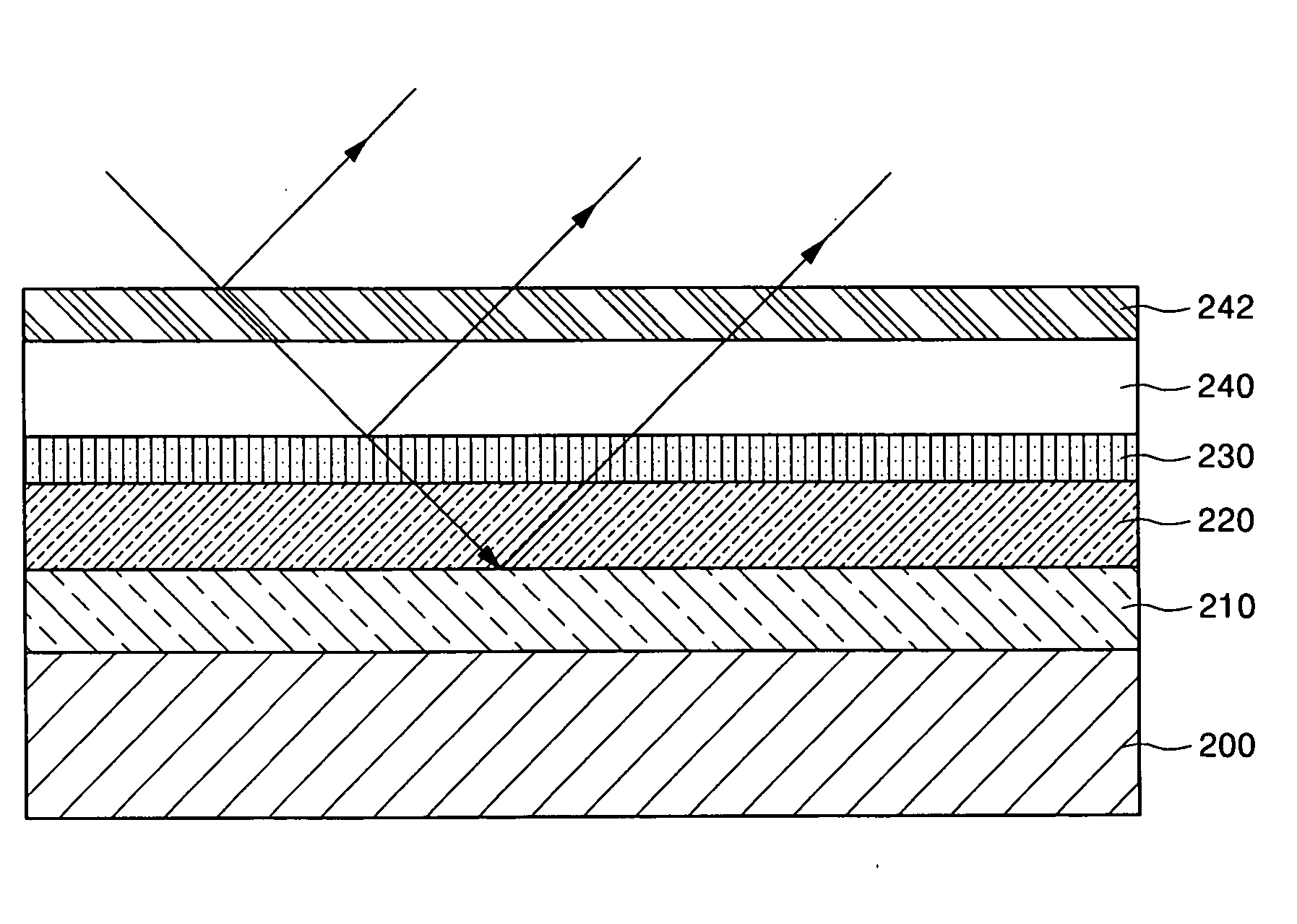
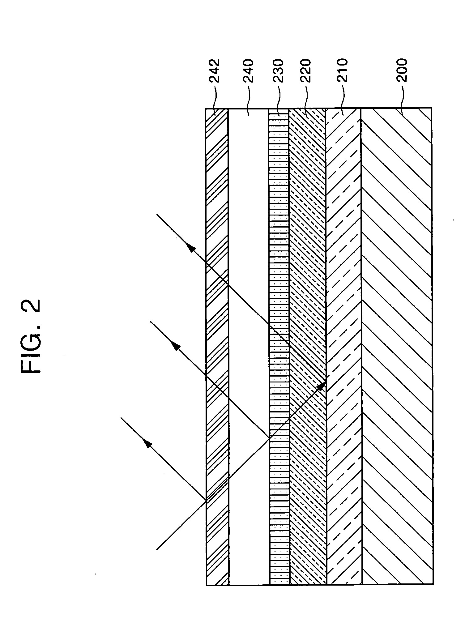
[0040] An OLED was formed as follows. A pixel electrode 210 was formed on a substrate 200. An organic emission layer 220 was formed on the pixel electrode 210. The organic emission layer 220 was made to different thicknesses according to its color. Red and green emission layers were 400 Å thick, and a blue emission layer was 150 Å thick. An electron transport layer about 250 Å to about 300 Å thick was formed as part of the emission layer. An opposite electrode 230, 180 Å thick was formed on the organic layer 220. A phase shift layer 240, 500 Å to 800 Å thick was formed on the opposite electrode 230. A reflecting layer 242, 80 Å to 120 Å thick was formed on the phase shift layer 240. The luminous efficiency of Embodiment 1 is shown in Table 1.


PUM


Abstract

A flat panel display includes a pixel electrode, an organic emission layer, an opposite electrode, a phase shift layer and a reflecting layer disposed on a substrate. The phase shift layer and the reflecting layer are stacked on the opposite electrode to destructively interfere with reflected external light to realize black and achieve excellent luminous efficiency.

Description

CROSS-REFERENCE TO RELATED APPLICATION [0001] This application claims priority to and the benefit of Korean Patent Application No. 10-2004-0098877, filed on Nov. 29, 2004, which is hereby incorporated by reference for all purposes as if fully set forth herein. BACKGROUND OF THE INVENTION [0002] 1. Field of the Invention [0003] This invention relates to a flat panel display that has a phase shift layer and a reflecting layer stacked on an opposite electrode to destructively interfere with reflected external light to realize black. The invention also relates to a method of fabricating the flat panel display. [0004] 2. Discussion of the Background [0005] An organic light emitting display (OLED) has a contrast ratio depending on the intensity of external light. A black matrix material may be employed to improve the contrast ratio, but it is very difficult to realize perfect black by shielding the external light in an emission region. [0006] One device used in the prior art to attempt to...

Claims


Application Information

Patent Timeline
Patent Type & Authority Applications(United States)
IPC IPC(8): H01L29/08
CPCH01L27/32H01L51/5265H01L51/5281H10K59/00H10K50/852H10K50/86H05B33/22H05B33/26
Inventor LEE, KWAN-HEEIM, JA-HYUN
Owner SAMSUNG DISPLAY CO LTD
Why Eureka
Try Eureka