

Plasma ion implantation system with axial electrostatic confinement
a technology of plasma ion implantation and axial electrostatic confinement, which is applied in the direction of vacuum evaporation coating, chemical vapor deposition coating, coating, etc., can solve the problems of increasing the risk of arcing within the plasma doping chamber, increasing the gas pressure, and/or lowering the gas pressur
- Summary
- Abstract
- Description
- Claims
- Application Information
AI Technical Summary
Problems solved by technology
Method used
Image

Examples
first embodiment
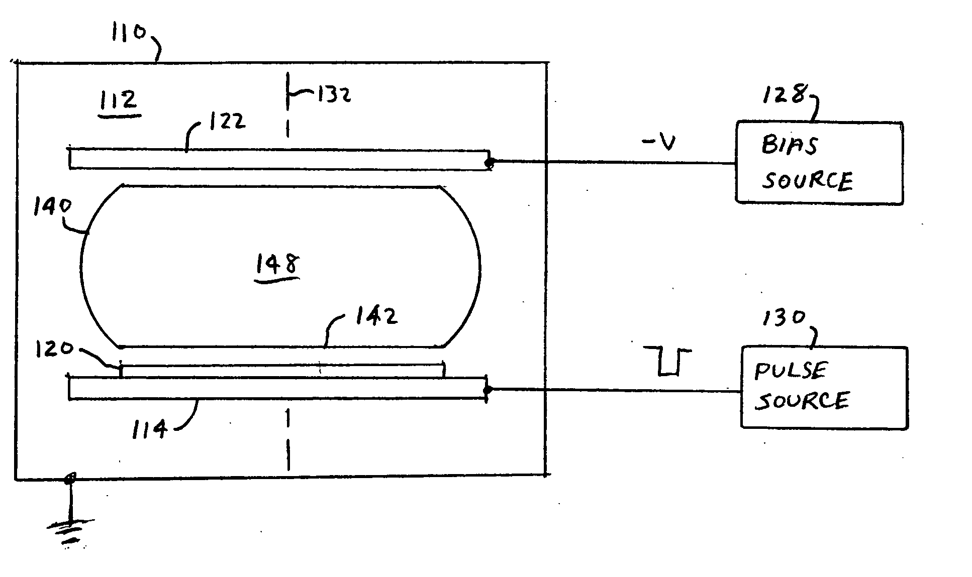
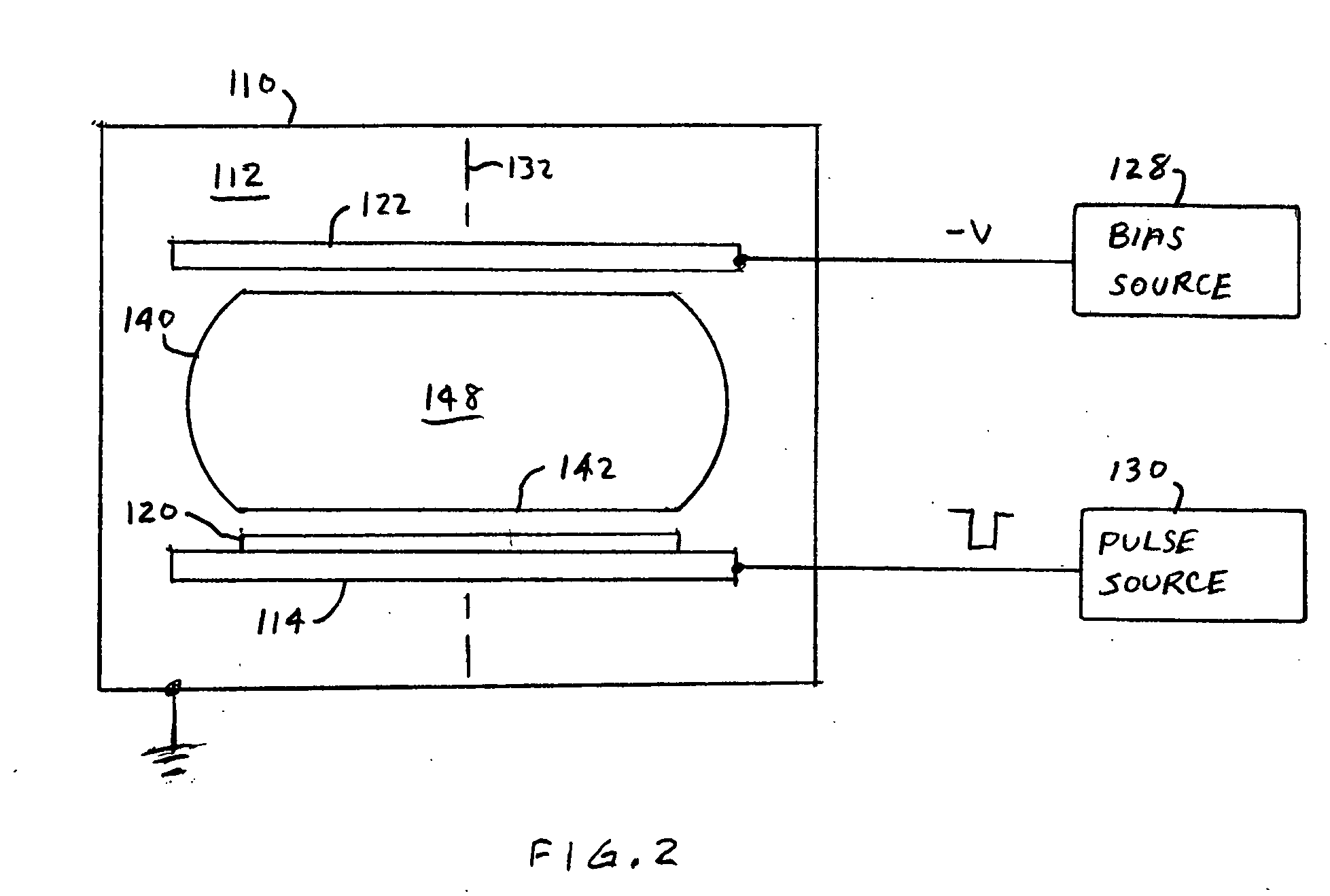
[0029] A simplified schematic block diagram of a plasma ion implantation system in accordance with the invention is shown in FIG. 2. As shown in FIG. 2, a process chamber 100 defines an enclosed volume 112. A platen 114 positioned within chamber 100 provides a surface for holding a substrate, such as a semiconductor wafer 120. Platen 114 is connected to a pulse source 130, and process chamber 110 is connected to ground. Platen 114 functions as a cathode, and process chamber 110 functions as an anode. Pulse source 130 applies to platen 114 negative implant pulses, as described above in connection with pulse source 30.
[0030] An auxiliary electrode 122 is positioned within chamber 110 in spaced relation to platen 114. Auxiliary electrode 122 may be movable in a direction perpendicular to platen 114. In general, auxiliary electrode 122 may be parallel to and spaced from platen 114 and may have the same physical configuration as anode 24 shown in FIG. 1 and described above. Auxiliary ele...
second embodiment
[0034] A simplified schematic block diagram of a plasma ion implantation system in accordance with the invention is shown in FIG. 3. The embodiment of FIG. 3 differs from the embodiment of FIG. 2 in that the pulse source 130 is connected to both platen 114 and auxiliary electrode 122. Thus, the implant pulses supplied to platen 114 are also applied to auxiliary electrode 122. Because negative voltages are applied to electrodes 114 and 122, electrons are axially confined along axis 132 orthogonal to the wafer support surface of platen 114. The embodiment of FIG. 3 has the advantage that a single pulse source can be utilized to energize platen 114 and auxiliary electrode 122. However, this configuration has the disadvantage that independent control of auxiliary electrode 122 is lacking.
third embodiment
[0035] A simplified schematic block diagram of a plasma ion implantation system in accordance with the invention is shown in FIG. 4. In the embodiment of FIG. 4, pulse source 130 is connected to platen 114 and an auxiliary pulse source 150 is connected to auxiliary electrode 122. Pulse source 130 supplies to platen 114 negative implant pulses having a pulse amplitude, a pulse width and a pulse repetition rate selected to perform a desired implantation of dopant ions into wafer 120. Auxiliary pulse source 150 supplies to auxiliary electrode 122 negative auxiliary pulses having an amplitude selected to provide a desired density of plasma 140. The pulse width and pulse repetition rate may match the pulse width and pulse repetition rate of the pulses supplied by pulse source 130. In other embodiments, described below, the pulse widths may be different. Pulse sources 130 and 150 may be controlled by a synchronization device 160 which causes the pulses supplied to platen 114 and auxiliary...
PUM
 Abstract
Description
Claims
Application Information