Plasma accelerating apparatus and plasma processing system having the same

a technology of plasma processing and accelerating apparatus, which is applied in the direction of plasma technique, vacuum evaporation coating, coating, etc., can solve the problems of non-uniform etching profile formation, significant damage to cathode electrode b, /b>, etc., and achieve the effect of reducing an induction magnetic field

Active Publication Date: 2006-12-21
SAMSUNG ELECTRONICS CO LTD
View PDF5 Cites 8 Cited by
  • Summary
  • Abstract
  • Description
  • Claims
  • Application Information

AI Technical Summary

Benefits of technology

[0028] The plasma generating and accelerating portion may include an upper inductor disposed at an outer periphery in an axial direction of the end wall of the channel; an inner inductor located at a radial inside of the inner wall to reduce an

Problems solved by technology

Furthermore, the Hall effect plasma accelerating apparatus 10 laminates a charge on a surface of a substrate on which ions are deposited, causing a loss such as a charge shunt and notching to occur in a minute pattern that may lead to a formation of a non-uniform etching profile.
The cathode electrode 54 is significantly damaged through the coll

Method used


Image

  • Plasma accelerating apparatus and plasma processing system having the same
  • Plasma accelerating apparatus and plasma processing system having the same
  • Plasma accelerating apparatus and plasma processing system having the same

Examples


Embodiment Construction

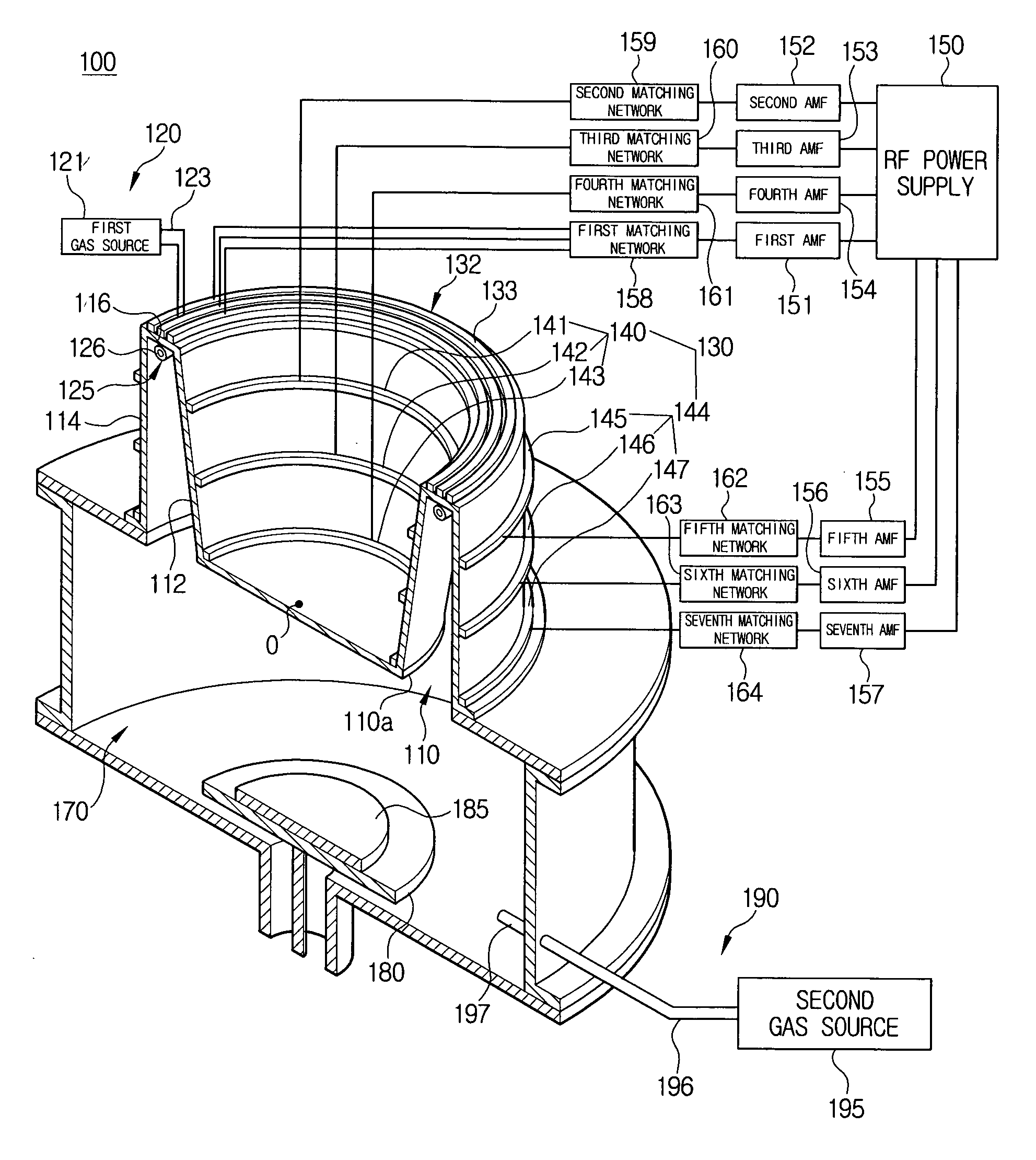
[0044] Hereinafter, a plasma accelerating apparatus and a plasma processing system including the plasma accelerating apparatus according to an exemplary embodiment of the present invention will be described with reference to accompanying drawings in detail.

[0045]FIG. 6 is a schematic cut-away perspective view showing a plasma processing system 100 including a plasma accelerating apparatus according to an exemplary embodiment of the present invention.

[0046] The plasma processing system 100 of the present invention is a plasma etcher that forms a selective etching pattern on a substrate 185 by evaporating or ashing, a thin film such as photoresist coated on the substrate using high temperature ionized plasma to remove it therefrom.

[0047] With reference to FIG. 6, the plasma processing system 100 includes a plasma channel 110, a first gas supply portion 120, a plasma generating and accelerating portion 130, a process chamber 170, and a second gas supply portion 190. The plasma chann...


PUM

PropertyMeasurementUnit
Angleaaaaaaaaaa
Magnetic fieldaaaaaaaaaa
Currentaaaaaaaaaa

Abstract

A plasma accelerating apparatus and a plasma processing system having the same are provided. The apparatus includes a circular channel comprising an inner wall, an outer wall, and an end wall connected to an end of the inner wall and the outer wall to form an outlet port at the other ends of the inner and outer walls; a gas supply portion to supply a gas to an inside of the channel; and a plasma generating and accelerating portion to supply ionization energy to the gas inside the channel to generate a plasma beam, and to accelerate the generated plasma beam toward the outlet port, wherein one of the inner wall and outer wall of the channel is inclined at an angle so that the other end of the wall is located closer to a center of the plasma accelerating apparatus.

Description

CROSS-REFERENCE TO RELATED APPLICATIONS [0001] This application claims priority from Korean Patent Application No. 10-2005-0052514 filed on Jun. 17, 2005 in the Korean Intellectual Property Office, the entire contents of which is incorporated herein by reference. BACKGROUND OF THE INVENTION [0002] 1. Field of the Invention [0003] The present invention relates to a plasma accelerating apparatus, and more particularly, to a plasma accelerating apparatus and a plasma processing system having the same, which is used for semiconductor substrate processing for etching and removing a thin film from a substrate or depositing the thin film on the substrate. [0004] 2. Description of the Related Art [0005] In recent years, with the increased need of high speed microprocessors and high recording density memories, a technique of reducing a thickness of a gate dielectric substance and a lateral size of a logic element has been actively developed so that many elements can be mounted on one semicon...

Claims


Application Information

Patent Timeline
IPC IPC(8): H01J7/24
CPCH01J37/321H05H1/54H01J37/32357H01L21/302
Inventor YOO, JIN-WOOPARK, WON-TAEK
Owner SAMSUNG ELECTRONICS CO LTD
Why Eureka
Try Eureka