In-situ deposition of film stacks

a technology of film stacks and film layers, applied in the direction of chemical vapor deposition coatings, coatings, plasma techniques, etc., can solve the problems of contaminating other process tools, contaminating devices, and device failures

Active Publication Date: 2015-05-12
NOVELLUS SYSTEMS
View PDF78 Cites 5 Cited by
  • Summary
  • Abstract
  • Description
  • Claims
  • Application Information

AI Technical Summary

Problems solved by technology

Some deposition processes generate small gas phase particles during process, which may decorate a deposition surface, potentially contaminating the device.
Such particles may cling to the device, potentially blocking subsequent etch and / or deposition events, which may ultimately lead to device failure.
Further, particles may be knocked off the device downstream, potentially contaminating other process tools.
However, such approaches may diminish film deposition rates, requiring the installation and maintenance of additional process tools to support a production line.
Further, films produced by such approaches may have physical or electrical characteristics that provide inadequate device performance.
Further still, such approaches may not address particles formed in various exhaust hardware for the process tool, which may back-stream and contaminate the device.
Once coated by additional film material, the small size of the particles may be magnified, causing ripples and distortions at the film surface.
These ripples may make it difficult to pattern the resulting films.
Patterning problems may also be caused by rough films.
Some traditional atomic layer deposition (ALD), chemical vapor deposition (CVD), high-density plasma chemical vapor deposition (HDP-CVD) and plasma-enhanced chemical vapor deposition (PECVD) processes for depositing film layers may produce unacceptably rough films, cause unacceptable interfacial mixing between film layers, and may have interfacial defects caused by vacuum breaks between successively deposited film layers.
The resulting rough film interfaces and interfacial defects may be magnified by subsequently deposited layers as the film stack is built, so that the top surface of the film stack may be unacceptably rough for downstream patterning processes.
Further, interfacial defects within the film stack may lead to structural and / or electrical defects in the resulting integrated device.

Method used


Image

  • In-situ deposition of film stacks
  • In-situ deposition of film stacks
  • In-situ deposition of film stacks

Examples


example

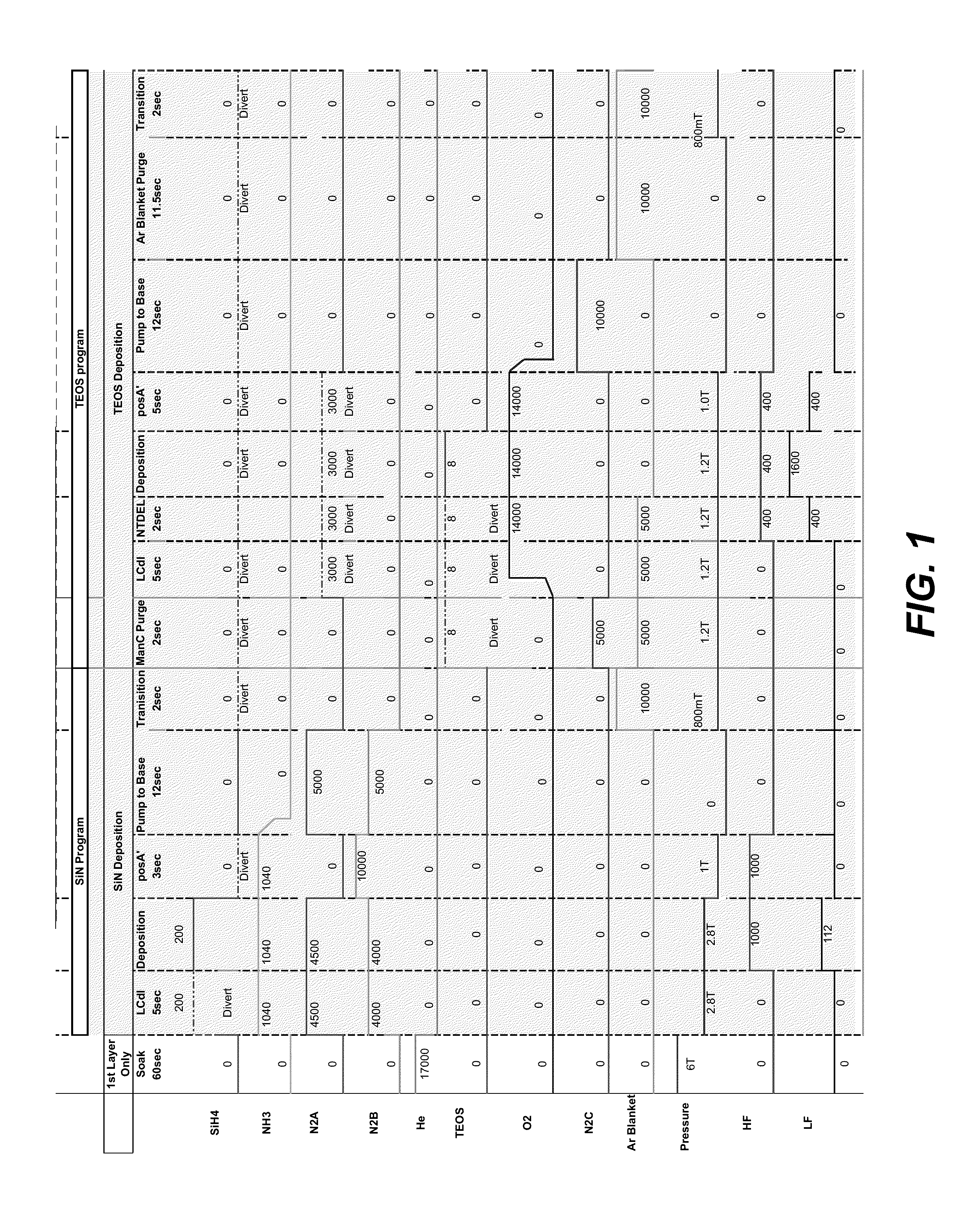
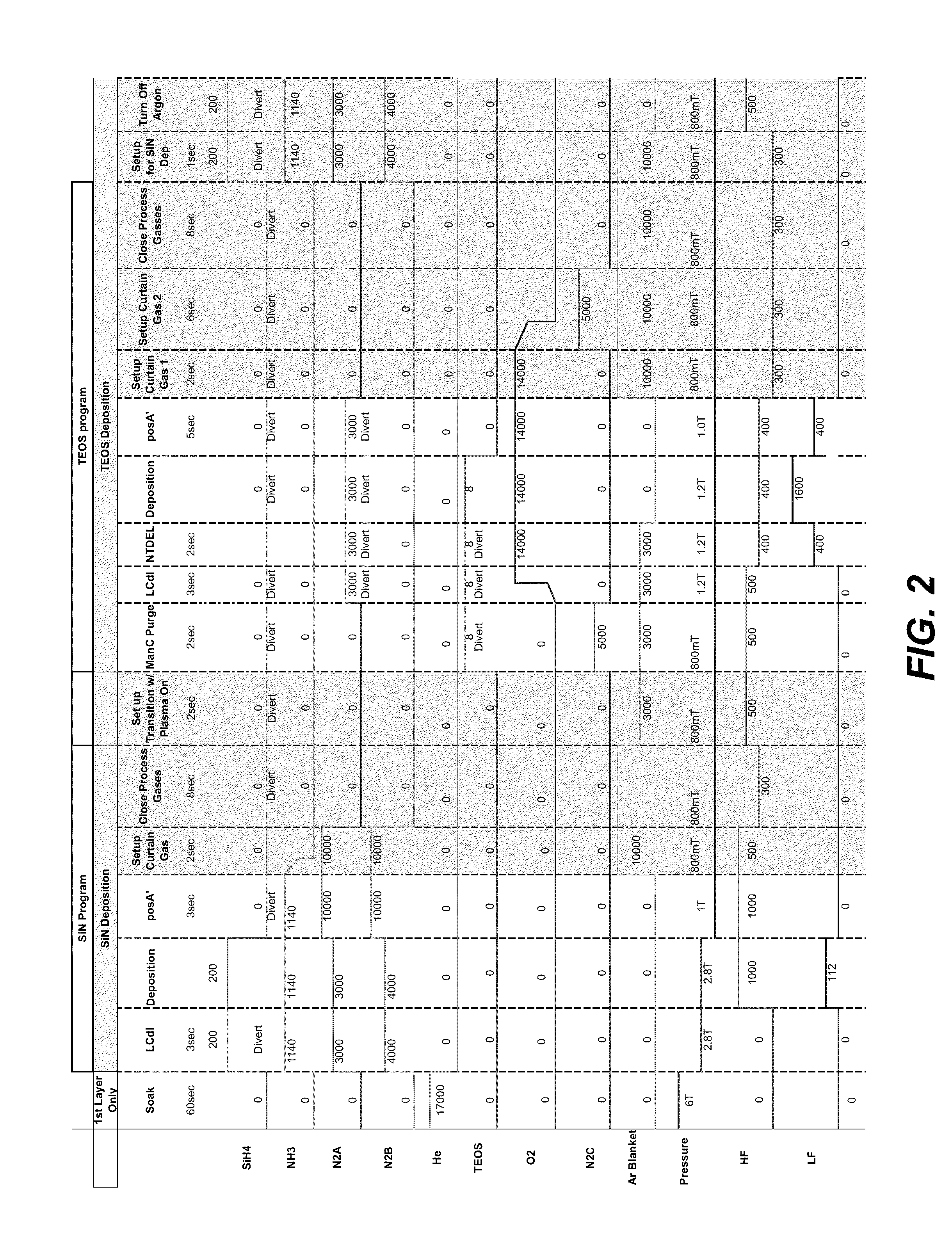
[0063]To compare the continuous plasma on (CPO) process with the reference pump-to-base (PTB) process, film stacks having alternating layers of silicon nitride and silicon oxide (SiN / SiOx stacks) were formed using both the reference PTB process of FIG. 1 and the CPO process of FIG. 2. The SiN / SiOx stacks were formed on 14 pairs of wafers for each process so that average stack defect count and total processing time could be compared. It is estimated that the stacks comprised 300 Å of silicon oxide (formed from TEOS precursor) and 500 Å of silicon nitride, except that: the 1st pair of wafers is estimated to have comprised 1300 Å of SiOx, the 2nd to have comprised 1000 Å of SiOx, the 12th to have comprised 1300 Å of SiOx, and the 14th pair of wafers to have comprised 2300 Å of SiOx.

[0064]The wafers were processed in batches, the stack defects in each batch counted, the total batch cycle times accumulated, and the results are listed in TABLE 1 below. Note that a stack defect is essentia...


PUM

PropertyMeasurementUnit
pressureaaaaaaaaaa
frequenciesaaaaaaaaaa

Abstract

Methods of forming a film stack may include the plasma accelerated deposition of a silicon nitride film formed from the reaction of nitrogen containing precursor with silicon containing precursor, the plasma accelerated substantial elimination of silicon containing precursor from the processing chamber, the plasma accelerated deposition of a silicon oxide film atop the silicon nitride film formed from the reaction of silicon containing precursor with oxidant, and the plasma accelerated substantial elimination of oxidant from the processing chamber. Process station apparatuses for forming a film stack of silicon nitride and silicon oxide films may include a processing chamber, one or more gas delivery lines, one or more RF generators, and a system controller having machine-readable media with instructions for operating the one or more gas delivery lines, and the one or more RF generators.

Description

CROSS REFERENCE TO RELATED APPLICATIONS[0001]This application is a continuation-in-part of, and claims priority to, U.S. patent application Ser. No. 12 / 970,846, filed Dec. 16, 2010, and titled “IN-SITU DEPOSITION OF FILM STACKS,” which claims priority to: U.S. Provisional Patent Application No. 61 / 317,656, filed Mar. 25, 2010 and titled “IN-SITU PLASMA-ENHANCED CHEMICAL VAPOR DEPOSITION OF FILM STACKS”; U.S. Provisional Patent Application No. 61 / 382,465, filed Sep. 13, 2010, and titled “IN-SITU PLASMA-ENHANCED CHEMICAL VAPOR DEPOSITION OF FILM STACKS”; U.S. Provisional Patent Application No. 61 / 382,468, filed Sep. 13, 2010, and titled ‘SMOOTH SILANE-BASED FILMS”; and U.S. Provisional Patent Application No. 61 / 394,707, filed Oct. 19, 2010, and titled “IN-SITU PLASMA-ENHANCED CHEMICAL VAPOR DEPOSITION OF FILM STACKS.” Each of the foregoing provisional and non-provisional applications are hereby incorporated by reference herein in their entirety for all purposes.BACKGROUND[0002]Various...

Claims


Application Information

Patent Timeline
Patent Type & Authority Patents(United States)
IPC IPC(8): C23C16/44C23C16/34C23C16/455H05H1/24C23C16/54H01L21/02C23C16/40C23C16/24C23C16/509
CPCC23C16/24C23C16/509C23C16/4401C23C16/45523C23C16/402C23C16/54H01L21/02274H01L21/02123H01L21/0234C23C16/345H01L21/022H01L21/02164
Inventor HAVERKAMP, JASONSUBRAMONIUM, PRAMODWOMACK, JOENIU, DONGFOX, KEITHALEXY, JOHNBREILING, PATRICKO'LOUGHLIN, JENNIFERSRIRAM, MANDYAMANTONELLI, GEORGE ANDREWVAN SCHRAVENDIJK, BART
Owner NOVELLUS SYSTEMS
Why Eureka
Try Eureka