Methods for forming dual damascene wiring using porogen containing sacrificial via filler material

Inactive Publication Date: 2006-06-08
SAMSUNG ELECTRONICS CO LTD
View PDF16 Cites 67 Cited by
  • Summary
  • Abstract
  • Description
  • Claims
  • Application Information

AI Technical Summary

Benefits of technology

[0012] In general, exemplary embodiments of the invention include methods for fabricating dual damascene interconnect structures and, in particular, to dual damascene methods in which a sacrificial material containing porogen (a pore forming agent) is used

Problems solved by technology

However, copper is difficult to pattern using a conventional photolithography/etching techniques, especially when the copper wires are formed according to relatively small design rules.
Although dual damascene methods allow formation of metal interconnect structures that yield improved performance, such methods become more problematic with decreasing design rules.
For instance, with decreasing design rules, parasitic resistance and capacitance that exists between adjacent metal wiring layers in a lateral direction or in a vertical direction may affect the performance of the semiconductor devices.
Indeed, parasitic capacitance and resistance results in capacitive coupling and cross talk between adjacent metal lines, which decreases the performance.
Further, the parasitic resistance and capacitance components result in increased signal leakage and increased power consumption of the semiconductor device.
Although the use of low-k dielectric materials provides improved performance, ILD layers formed with such low-k dielectric materials are more susceptible to etching damage.
For instance, in the conventional process as described above, an ILD layer formed of a low-k dielectric material can be damaged (contaminated and/or undesirably etched) during removal of the via-filling sacrificial material.
Although the methods disclosed by Meagley may help to minimize damage

Method used


Image

  • Methods for forming dual damascene wiring using porogen containing sacrificial via filler material
  • Methods for forming dual damascene wiring using porogen containing sacrificial via filler material
  • Methods for forming dual damascene wiring using porogen containing sacrificial via filler material

Examples


Embodiment Construction

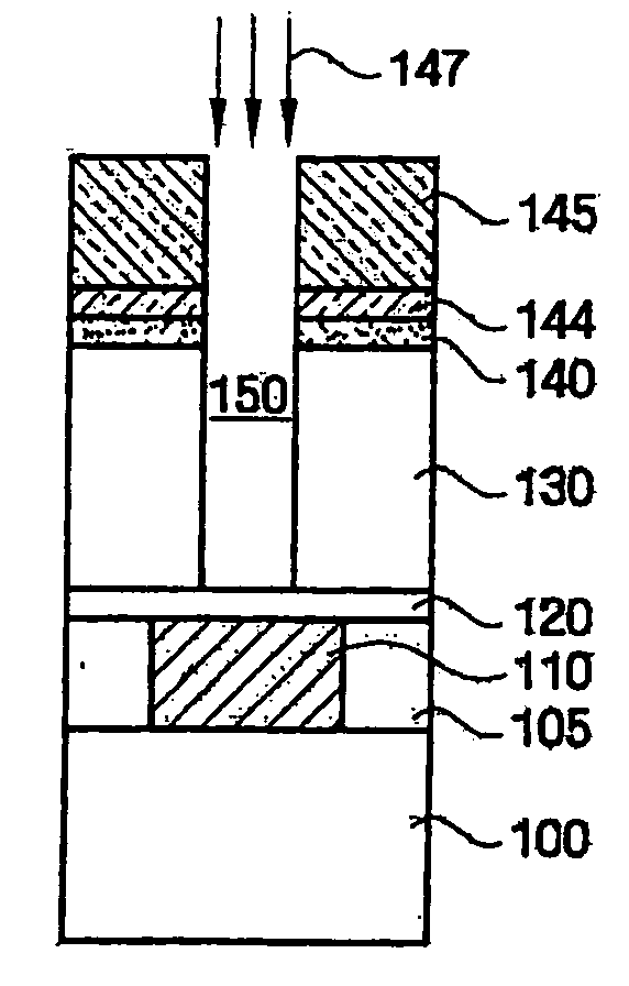
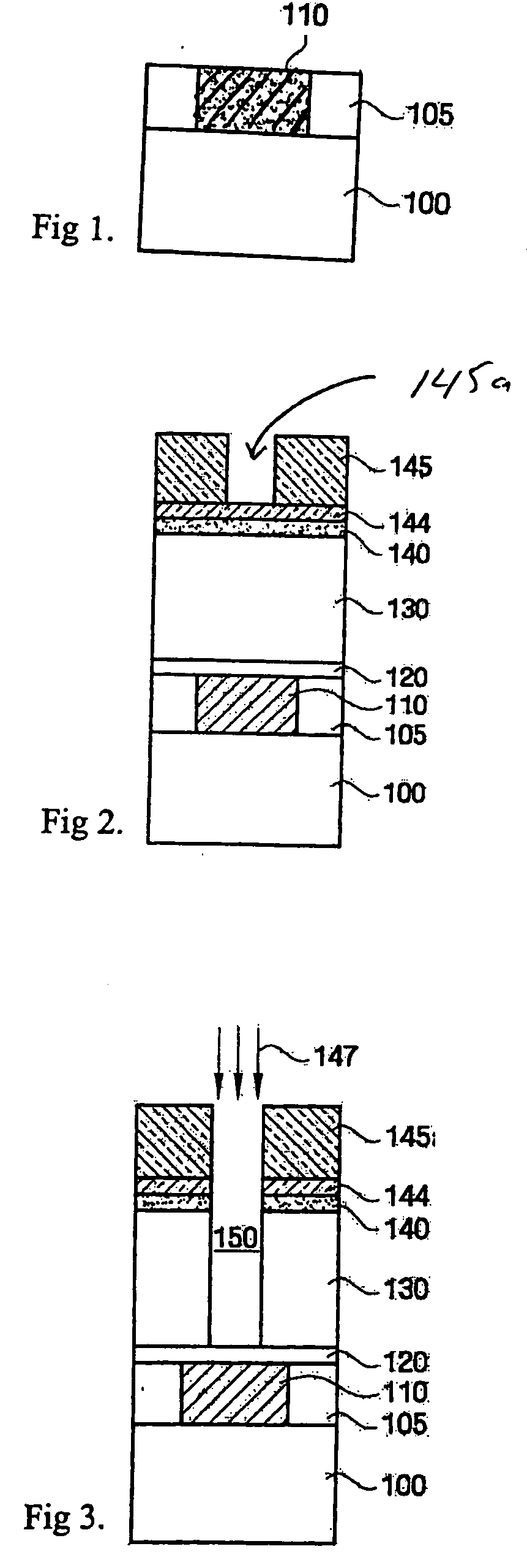
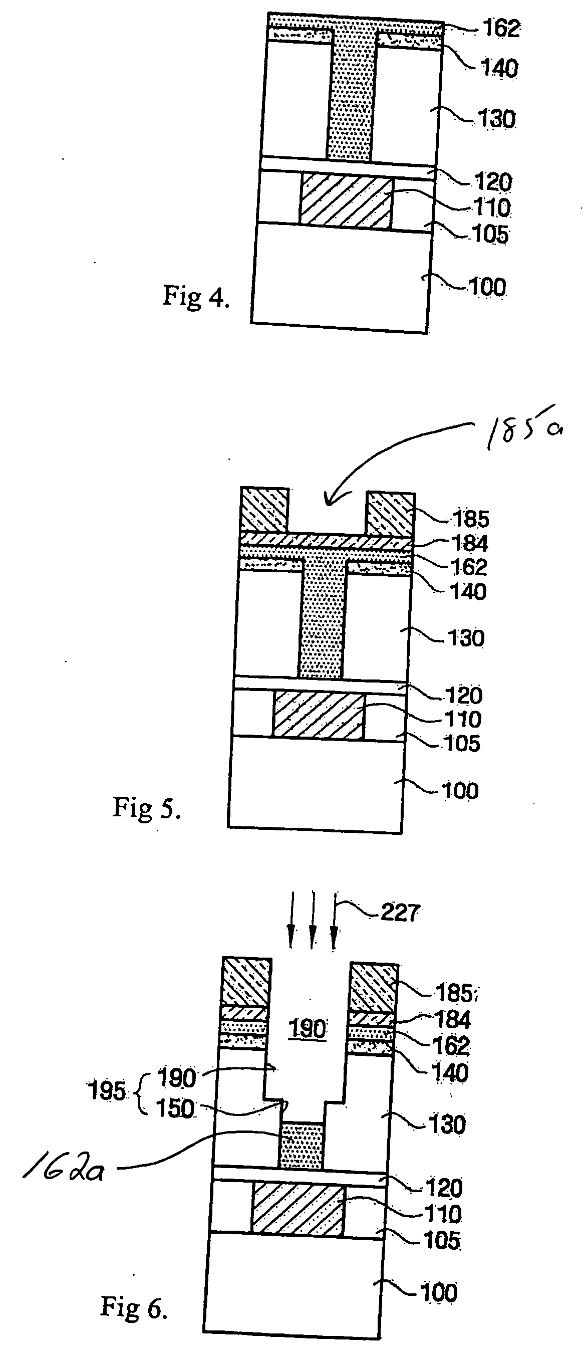
[0024] Exemplary embodiments of the invention will now be described more fully with reference to the accompanying drawings in which it is to be understood that the thickness and dimensions of the layers and regions are exaggerated for clarity. It is to be further understood that when a layer is described as being “on” or “over” another layer or substrate, such layer may be directly on the other layer or substrate, or intervening layers may also be present. Moreover, similar reference numerals used throughout the drawings denote elements having the same or similar functions.

[0025]FIGS. 1 through 9 are schematic cross-sectional views illustrating a method for forming a metal wiring layer of a semiconductor device according to an exemplary embodiment of the present invention. More specifically, FIGS. 1 through 9 illustrates a dual damascene method in which a sacrificial material containing porogen (a pore forming agent) is used for filling via holes in an interlayer dielectric layer s...


PUM


Abstract

Methods for fabricating dual damascene interconnect structures are provided in which a sacrificial material containing porogen (a pore forming agent) is used for filling via holes in an interlayer dielectric layer such that the sacrificial material can be transformed to porous material that can be quickly and efficiently removed from the via holes without damaging or removing the interlayer dielectric layer.

Description

CROSS-REFERENCE TO RELATED APPLICATION [0001] This application claims priority to Korean Patent Application No. 10-2004-0103088, filed on Dec. 8, 2004, which is incorporated herein by reference. TECHNICAL FIELD [0002] The present invention relates generally to methods for fabricating dual damascene interconnect structures and, in particular, to dual damascene methods in which a sacrificial material containing porogen (a pore forming agent) is used for filling via holes in an interlayer dielectric layer such that the sacrificial material can be transformed to porous material that can be readily removed from the via holes without damaging or removing the interlayer dielectric layer. BACKGROUND [0003] Due to continued technological innovations in the field of semiconductor fabrication which allow integrated circuits to be designed according to smaller design rules (DR), semiconductor devices are becoming more highly integrated. Typically, highly integrated circuits are designed using m...

Claims


Application Information

Patent Timeline
IPC IPC(8): H01L21/4763
CPCH01L21/76808H01L21/28B82Y40/00
Inventor LEE, KYOUNG WOOSHIN, HONG JAEKIM, JAE HAK
Owner SAMSUNG ELECTRONICS CO LTD
Why Eureka
Try Eureka