Solder reflow system and method thereof

Inactive Publication Date: 2006-06-15
IBM CORP
View PDF10 Cites 14 Cited by
  • Summary
  • Abstract
  • Description
  • Claims
  • Application Information

AI Technical Summary

Benefits of technology

[0010] An aspect of this invention is that it satisfactorily addresses problems of controlling solder reflow of microelectronic assemblies while preventing degradation to components surrounding the mi

Problems solved by technology

However, some semiconductors are not satisfactorily bonded in the process and/or might be otherwise be damaged.
Without the ability to effectively heat the lead-free solder-based materials, an

Method used


Image

  • Solder reflow system and method thereof
  • Solder reflow system and method thereof
  • Solder reflow system and method thereof

Examples


Embodiment Construction

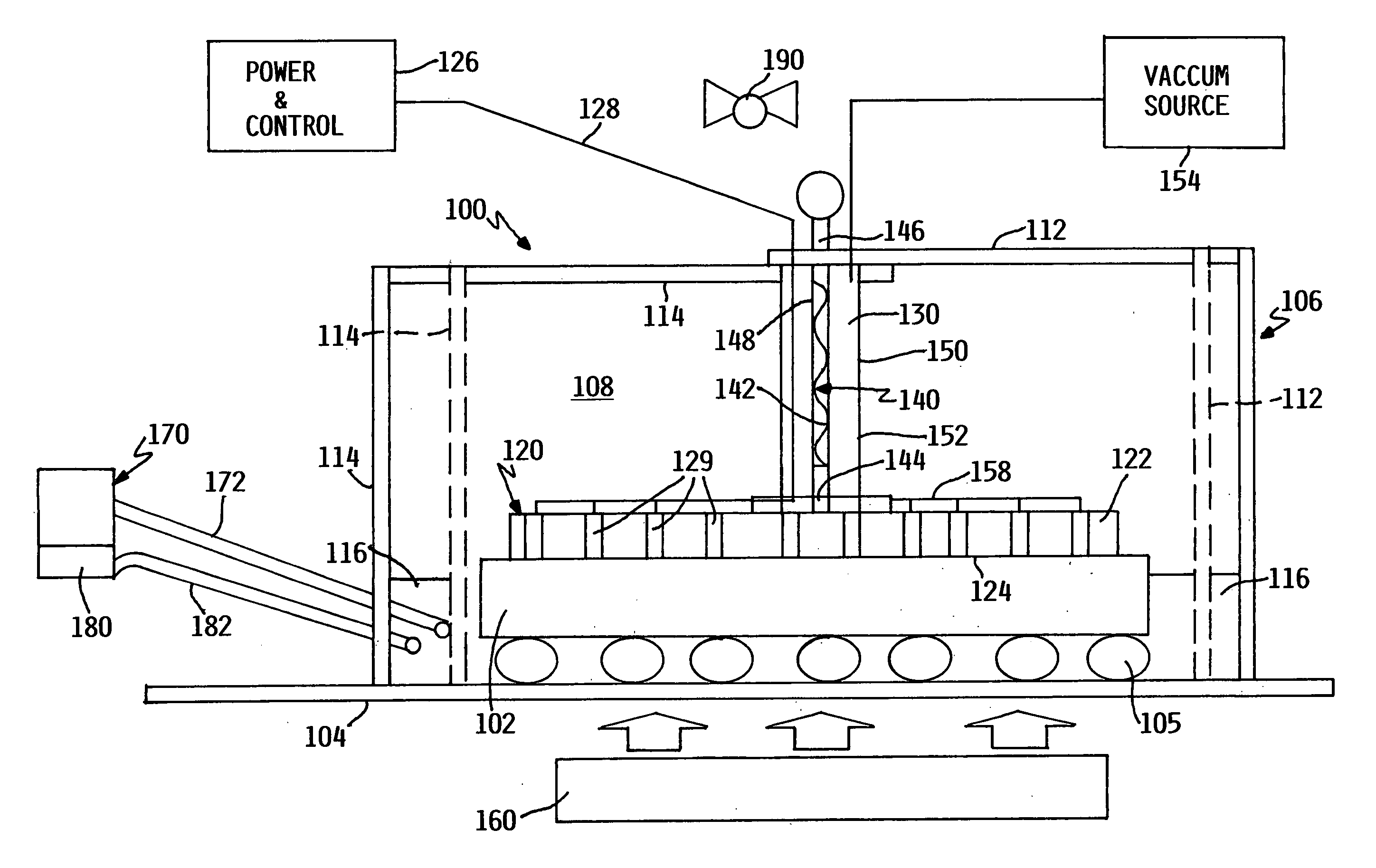
[0015] Reference is made is made to FIGS. 1 & 2 for illustrating one preferred embodiment of a solder reflow heating system 100 that is adapted for use in implementing a solder reflow process. The solder reflow heating system 100 operates to efficiently effect solder reflow without the permitting degradation to microelectronic assemblies subject to the reflow process and those objects immediately surrounding the former.

[0016] The solder reflow heating system 100 is versatile in that it may adapted to encapsulate one or more microelectronic assemblies or microelectronic assemblies 102 (only one is shown) that are solder mounted via solder balls 105 on a substrate 104. In this embodiment, the substrate 104 is a printed circuit board 104 that may be any conventional board on which the heat-producing electronic / electrical microelectronic assemblies 102 are mounted. For instance, the circuit board 104 may be a printed wiring board (“PWB”) of the type commonly used in a PC. In addition, ...


PUM

PropertyMeasurementUnit
Forceaaaaaaaaaa
Sizeaaaaaaaaaa
Volumeaaaaaaaaaa

Abstract

A reflow heating system includes a housing assembly defining an internal thermal processing chamber that encapsulates at least a microelectronic assembly on a substrate. A first heating source is coupled to the housing assembly and within the thermal processing chamber. The first heating source is biased by a force-applying assembly into engagement with the microelectronic assembly. The first heating source comprises one or more heating platens adapted to engage the microelectronic assembly for applying direct heat sufficient to melt solder. A vacuum assembly is incorporated in the heating platen for allowing application of at least a partial vacuum to the microelectronic assembly to permit withdrawal thereof from the substrate. A radiant heating source is applied beneath the substrate and a directional heating source is applied to the microelectronic assembly.

Description

BACKGROUND [0001] The present invention relates generally to an improved heating system and method of controlling a solder reflow process. [0002] Printed circuit boards are commonly fabricated using the reflow solder technique. Many modern semiconductor devices are constructed to be attached to a higher level of assembly by means of solder balls. Solder balls are formed on the surface of the substrate forming the semiconductor device. Typically, those solder balls are formed on contact pads on the surface of a substrate, as those contact pads form the external connection with the internal circuitry of the substrate. [0003] However, some semiconductors are not satisfactorily bonded in the process and / or might be otherwise be damaged. Therefore, a need exists for a method of replacement or remounting. As a result, they are removed and re-soldered to the board. Because of environmental concerns regarding the use of lead in conventional soldering materials, there is a continuing trend t...

Claims


Application Information

Patent Timeline
IPC IPC(8): B23K31/02
CPCB23K1/005B23K2201/40H05K3/3494H05K2201/10734H05K2203/0195H05K2203/0278H05K2203/081H05K2203/1572H05K2203/1581B23K2101/40
Inventor KUCZYNSKI, JOSEPHSINHA, ARVIND KUMARTOFIL, TIMOTHY JEROME
Owner IBM CORP
Why Eureka
Try Eureka