Scanning interference electron microscope

an electron microscope and scanning interference technology, applied in the field of scanning interference electron microscopes, can solve the problems of complex and difficult adjustment, low detection efficiency of electron beams, etc., and achieve the effects of improving detection sensitivity or detection precision, high sensitiveness, and easy adjustment and adjustmen

Inactive Publication Date: 2006-06-15
HITACHI HIGH-TECH CORP
View PDF3 Cites 22 Cited by
  • Summary
  • Abstract
  • Description
  • Claims
  • Application Information

AI Technical Summary

Benefits of technology

[0013] Regarding a problem described in the above (2), since only one detector is used, it is essential to select and display either the amplitude image corresponding to a normal electron microscope image or the phase image, thus simultaneous display being impossible. If the observer is enabled to observe simultaneously structure information obtained from the normal electron microscope image and electromagnetic field information obtained from the phase image, it will give the observer an extra convenience.
[0014] The above (3) results from a fact that, since electron beams passing through the slit are allowed to enter the detector, a part of the electron beam blocked by the slit is not used. Since the electron beams blocked the slit cannot be used effectively, there is a limit in improving detection sensitivity or detection precision. Although it is possible to capture the whole image of the interference fringes, namely, to detect all the electrons, and process them with a high-speed processor, a time to transfer data to the processor, a time required for arithmetic computing, a time to transfer the data to memory, etc. will become huge, which deprives the STEM type interference electron microscopy of its advantage that a phase image can be displayed real-time. The present invention has its object to provide a scanning interference electron microscope which is easy to set up and adjust and yet highly sensitive.
[0015] The present invention solves the above-mentioned problems by detecting interference fringes of electron beam with an electron beam detector that consists of one pair of multi pixels. That is, an output of this detector is a 1-dimensional interference fringe image such that a value of each pixel is an integration value of 2-dimensional pixels along one 1-dimensional direction. Moreover, in the present invention, by mounting this detector on an externally controllable rotationable stage, a magnification of the interference fringes and a rotation direction of the detector are automatically adjusted, so that the interference fringes can be detected under conditions of highest efficiency.
[0016] According to the present invention, the apparatus can detect interference fringes of the electron beams with an asymmetric 2-dimensional detector with integration capability, and adjust them at high-speed and easily, thereby being able to detect them under optimum conditions. Therefore, a scan image of a high S / N ratio can be obtained. Moreover, the use of one pair of detectors enables simultaneous display of the amplitude image and the phase image. Furthermore, unlike the conventional microscopes, this microscope uses no slit, and accordingly the whole electrons constituting the interference fringes can be used, achieving high detection efficiency.

Problems solved by technology

(1) Setting and adjustment are complex and difficult to do.
(2) Simultaneous display of a phase image and an amplitude image cannot be performed.
(3) The detection efficiency of the electron beams is low.
The above (1) problem arises from a fact that a relative direction between the slit and the interference fringes and positions thereof are adjusted manually.
Since the magnification weakens the intensity of interference fringes, the adjustment requires skills and experience and accurate adjustment is difficult.
Regarding a problem described in the above (2), since only one detector is used, it is essential to select and display either the amplitude image corresponding to a normal electron microscope image or the phase image, thus simultaneous display being impossible.
Since the electron beams blocked the slit cannot be used effectively, there is a limit in improving detection sensitivity or detection precision.

Method used


Image

  • Scanning interference electron microscope
  • Scanning interference electron microscope
  • Scanning interference electron microscope

Examples


first embodiment

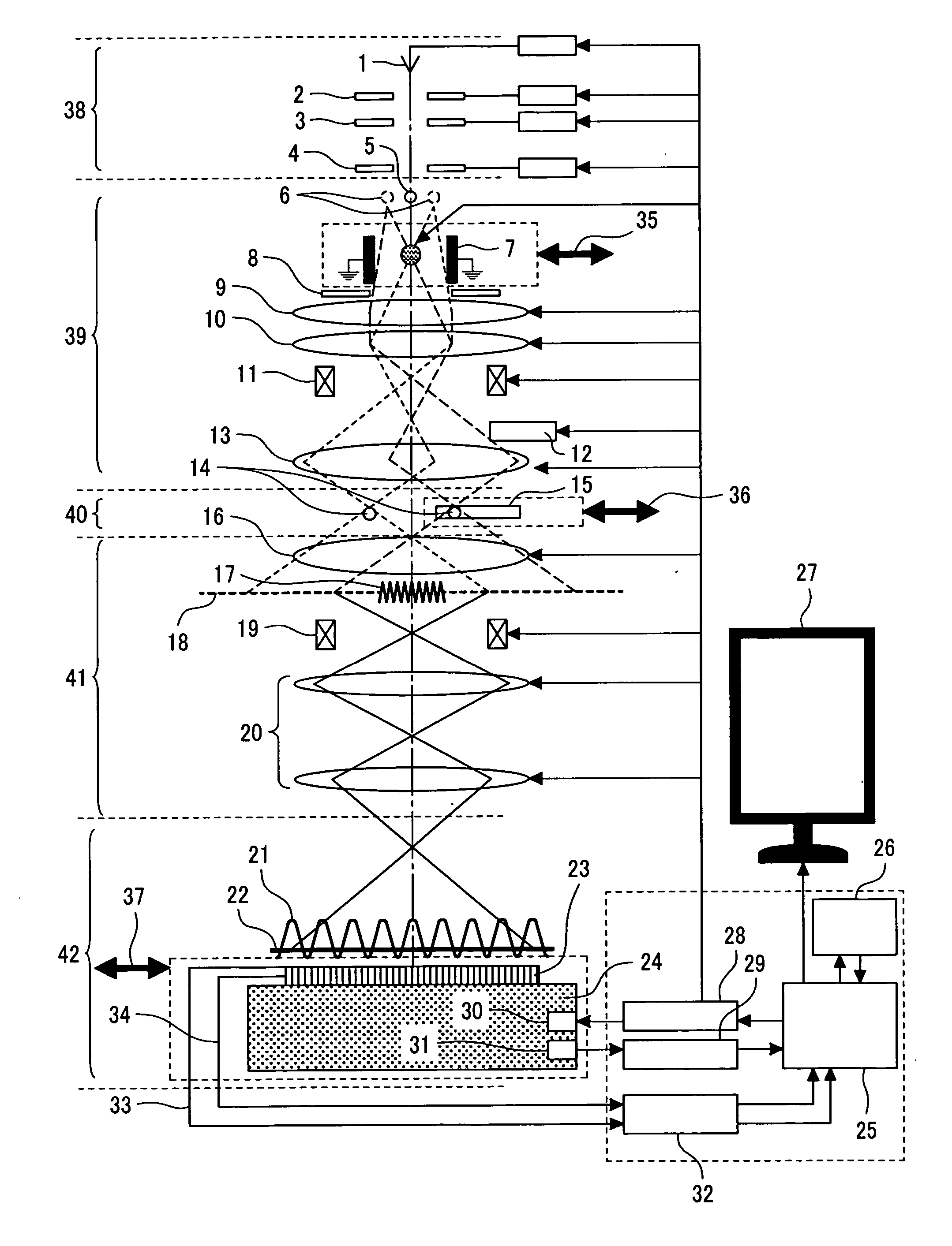
[0032] In this embodiment, an example where the present invention is applied to STEM will be described. FIG. 1 shows an example of a configuration of an STEM of this embodiment. The STEM of this embodiment comprises an electron gun 38, an illumination system 39, a specimen chamber 40, an imaging system 41, a detection system 42, a control system, etc., as a rough breakdown of the STEM.

[0033] The electron gun 38 of the STEM of this embodiment consists of an electron source 1, a first anode 2, a second anode 3, an acceleration anode 4, etc. The illumination system 39 consists of an electron biprism 7, a condenser aperture 8, a first condenser lens 19, a second condenser lens 10, a scanning coil 11, an objective lens pre-field 13, an objective lens post-field 16, etc. In addition, although not illustrated specifically, the electron biprism 7 is equipped with an electron biprism fine positioning system 35, and is made movable by this. The imaging system 41 and the detection system 42 c...

second embodiment

[0063]FIGS. 8A to 8D show another example of this embodiment. In this example, this embodiment is applied to dopant profile evaluation of a semi-conductor transistor. First, a voltage is applied to the electron biprism in the absence of specimen, the interference fringes magnified with an imaging lens is made to be incident on the asymmetric 2-dimensional detector with integration capability. After that, the electron beams are deflected with a deflection coil, and thereby the electron beams take an arrangement as shown in FIG. 8A. Here, one of two splitted electron beam spots 98, 99 is adjusted to pass through a vacuum and the other is adjusted to transmit through the specimen. Next, the two splitted electron beam spots are scanned in a direction of scanning 100, and at each predetermined scanning distance, the interference fringes are acquired. FIG. 8B shows a comparative relation between the specimen and the electron beam spot at the time when the electron beam is scanned as far a...

third embodiment

[0064]FIGS. 9A to 9D show further another example of the embodiment. In this, the STEM is applied to magnetic domain structure evaluation of a magnetic thin film. First, in the absence of specimen, a voltage is applied to the electron biprism and interference fringes magnified with an imaging lens are made to be incident on the asymmetric 2-dimensional detector with integration capability. After that, by deflecting the electron beam with a deflection coil, the electron beams take an arrangement as shown in FIG. 9A. Here, two splitted electron beam spots 108, 109 are so adjusted that one of them passes through a vacuum in proximity to the specimen and the other transmits through the specimen.

[0065] Next, while the two splitted electron beam spots are being scanned in a direction of scanning 110, the interference fringes are acquired at each predetermined scanning distance. FIG. 9B shows a comparative relation between the specimen and an electron beam spot at a time when the electron...


PUM


Abstract

The conventional detection technique has the following problems in detecting interference fringes: (1) Setting and adjustment are complex and difficult to conduct; (2) A phase image and an amplitude image cannot be displayed simultaneously; and (3) Detection efficiency of electron beams is low. The invention provides a scanning interference electron microscope which is improved in detection efficiency of electron beam interference fringes, and enables the user to observe electric and magnetic information easily in a micro domain of a specimen as a scan image of a high S/N ratio under optimum conditions.

Description

CLAIM OF PRIORITY [0001] The present invention claims priority from Japanese application JP 2004-357539 filed on Dec. 10, 2004, the content of which is hereby incorporated by reference on to this application. FIELD OF THE INVENTION [0002] The present invention relates to an electron beam apparatus, such as an electron microscope, which measures an electromagnetic field in a matter or vacuum using interference of electron beams. BACKGROUND OF THE INVENTION [0003] The electron holography, or the electron interference microscopy, is a technique of quantitatively measuring an electromagnetic field in a matter or vacuum by measuring a phase shift of an electron beam caused by a specimen, and specifically a technique in which an electron beam generated in an electron source is splitted into a plurality of electron beams by an electron biprism, a splitted electron beam is made to enter the specimen, and the electron beam having transmitted through the specimen is detected, whereby an inter...

Claims


Application Information

Patent Timeline
Patent Type & Authority Applications(United States)
IPC IPC(8): G21K7/00
CPCG03H5/00H01J37/023H01J37/244H01J37/28H01J2237/1502H01J2237/1514H01J2237/225H01J2237/228H01J2237/2447H01J2237/24495H01J2237/24564H01J2237/2487H01J2237/2614H01J2237/2802H01J2237/2803
Inventor MATSUMOTO, TAKAOKOGUCHI, MASANARI
Owner HITACHI HIGH-TECH CORP
Why Eureka
Try Eureka