Comparator for input voltages higher than supply voltage

a technology of input voltage and supply voltage, applied in the field of comparator, can solve the problems of high cost of higher power dissipation, battery cannot be integrated on the chip in standard technology, etc., and achieve the effect of limiting overvoltage and improving device performan

Active Publication Date: 2006-06-15
AMI SEMICON BELGIUM
View PDF11 Cites 20 Cited by
  • Summary
  • Abstract
  • Description
  • Claims
  • Application Information

AI Technical Summary

Benefits of technology

[0008] The comparator is implemented with a current mirror arrangement, but the additional reference voltage drop element enables higher voltages to be input and compared to an internal supply voltage level without the need for resistive dividers. The higher thresholds could be achieved by combining the conventional technique of a differential amplifier arrangement with the conventional voltage dropping resistive dividers on one or both inputs, but at a cost of higher power dissipation, i.e. due to the limitation imposed on the size of integrated resistors. The advantages are based on a recognition that the power dissipation of the comparator is determined by the biasing current sources only, and the area of semiconductor, e.g. silicon used by current sources is usually smaller than the area used by resistors of sufficient resistance to limit the current at the level imposed by these current sources. An additional advantage is that the inputs of the comparator are not connected to control electrodes of transistors, e.g. gates of MOS transistors, which should improve the resistance of the component to ESD. Hence the power dissipation and or the semiconductor, e.g. silicon area used can be kept lower than known arrangements using dividing resistors.
[0010] a diode or diodes in series. The diodes are forward biased but the use of reverse biased diodes is included, e.g. for very low currents, such as for use in the femto to nanoampere range. The advantages of diodes are their robustness and small size. This achieves one of the goals of the present invention, e.g. together with low power dissipation.
[0017] Another such feature is a third transistor in the first current path and coupled to the second main electrode, e.g. drain of the first transistor. The third transistor is connected between the first transistor and the current source in the first current path to limit the voltage at the positive electrode of the current source. A fourth transistor can be included in the second current path and coupled to a second main electrode, e.g. drain of the second transistor and the current source in the second current path to limit overvoltage at the positive electrode of the current source. Another such feature is circuitry coupled between the first main electrode, e.g. source, and a control electrode, e.g. gate of the second transistor to limit overvoltage. This is useful for enabling implementation in technologies vulnerable to such overvoltage. Another such feature is a diode coupled to the first input to protect the first input from current flow through forward biasing of a parasitic diode from drain to bulk of the first transistor.
[0018] Another aspect of the invention provides an integrated circuit having the comparator. Another aspect provides a battery powered mobile device having the integrated circuit. This is based on a recognition that the advantages of the integrated circuit can feed through to such devices to improve the device performance.

Problems solved by technology

The higher thresholds could be achieved by combining the conventional technique of a differential amplifier arrangement with the conventional voltage dropping resistive dividers on one or both inputs, but at a cost of higher power dissipation, i.e. due to the limitation imposed on the size of integrated resistors.
Typically, a battery cannot be integrated on chip in standard technologies.

Method used


Image

  • Comparator for input voltages higher than supply voltage
  • Comparator for input voltages higher than supply voltage
  • Comparator for input voltages higher than supply voltage

Examples


Embodiment Construction

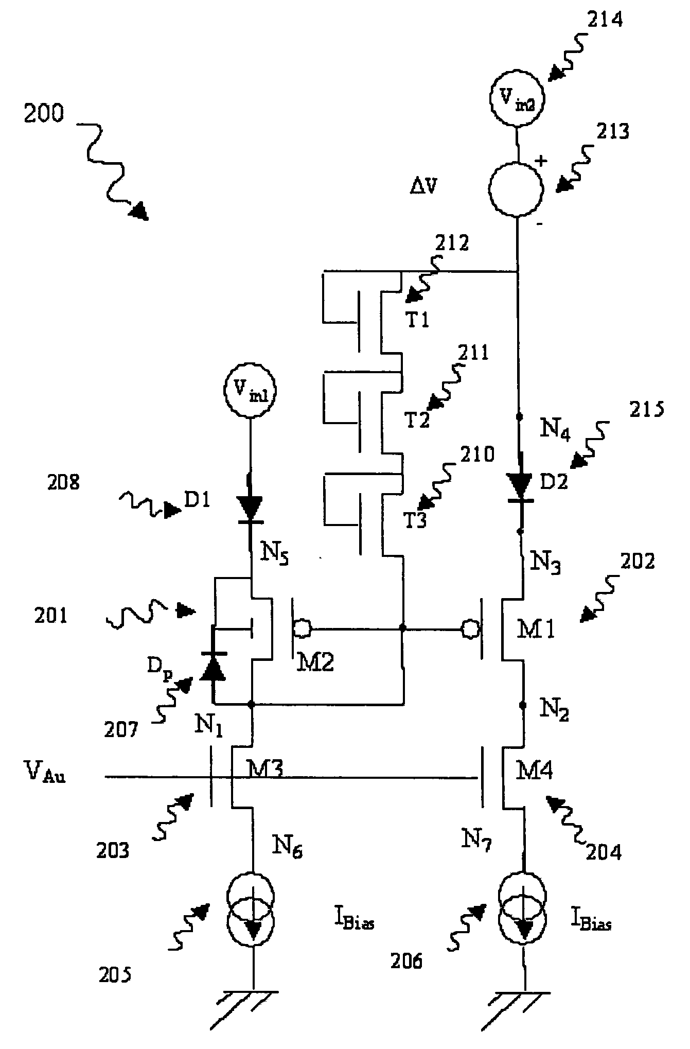
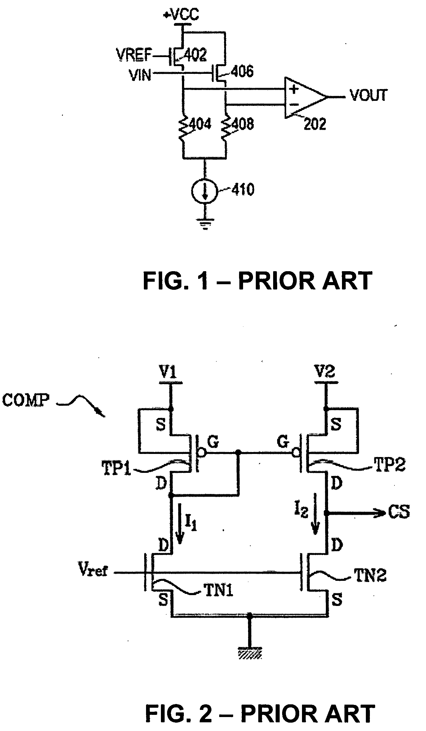
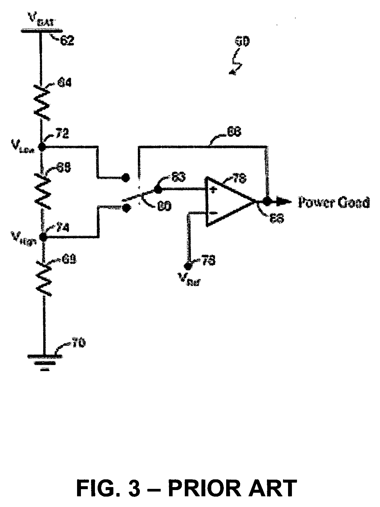
[0025] The present invention will be described with respect to particular embodiments and with reference to certain drawings but the invention is not limited thereto but only by the claims. Any reference signs in the claims shall not be construed as limiting the scope. The drawings described are only schematic and are non-limiting. In the drawings, the size of some of the elements may be exaggerated and not drawn on scale for illustrative purposes. Where the term “comprising” is used in the present description and claims, it does not exclude other elements or steps. Where an indefinite or definite article is used when referring to a singular noun e.g. “a” or “an”, “the”, this includes a plural of that noun unless something else is specifically stated.

[0026] It is furthermore to be noticed that the term “comprising”, used in the description and in the claims, should not be interpreted as being restricted to the means listed thereafter; it does not exclude other elements or steps. Th...


PUM


Abstract

A comparator has first and second current paths, each passing from an input through a transistor, through a current source to ground, the second current path also having a reference voltage drop element coupled in series with the second input. The gates of the transistors are coupled to form a current mirror. The reference voltage drop element enables higher voltages to be input and compared to higher thresholds above an internal supply voltage level without the need for dividing resistors to reduce the input voltage. Avoiding such resistors means the power dissipation and the silicon area used can be kept lower. ESD vulnerability is reduced since the inputs are not coupled to gates of MOS transistors. Overvoltage protection across the source and gate of the second transistor can be added.

Description

FIELD OF THE INVENTION [0001] This invention relates to comparators, and to integrated circuits having such comparators, and to devices having such integrated circuits as well as to methods of operating and making these. DESCRIPTION OF THE RELATED ART [0002] It is known to try to reduce power supply voltages for integrated circuits to reduce power consumption and to allow for increased integrated circuit densities. However, this may result in systems having integrated circuits using digital components powered by different supply voltages, which can cause interfacing problems. For example, transistors in the reduced voltage circuit may be subject to failure if forced to sustain the larger power supply voltage. If these transistors are protected with limiting diodes, this may prevent the transistors from detecting the desired signals, particularly in the case of differential signalling. Circuits such as comparators and differential amplifiers can use differential inputs. U.S. Pat. No....

Claims


Application Information

Patent Timeline
Patent Type & Authority Applications(United States)
IPC IPC(8): H03K5/22
CPCH03K5/08H03K5/2472
Inventor LAULANET, FRANCOISGENTINNE, BERNARD
Owner AMI SEMICON BELGIUM
Why Eureka
Try Eureka