Method for forming photoresist pattern and method for triming photoresist pattern

a photoresist pattern and pattern technology, applied in the field of photolithographic process, can solve the problems of poor resolution of the pattern transferred onto the photoresist layer, the difficulty of controlling the preciseness and uniformity of critical dimensions during the photolithographic process, and the uneven profile and rough surface of the patterned photoresist layer, etc., to achieve the effect of improving the smoothness of the profile and making the pattern of the photoresist layer more precis

Inactive Publication Date: 2006-06-15
UNITED MICROELECTRONICS CORP
View PDF5 Cites 1 Cited by
  • Summary
  • Abstract
  • Description
  • Claims
  • Application Information

AI Technical Summary

Benefits of technology

[0013] Accordingly, the present invention is to provide a method for forming a photoresist pattern so as to improve the smoothness of the profile of the patterned photoresist layer, and thus to make the pattern of the photoresist layer more precise.
[0014] The present invention is also to provide a method for multiply trimming the photoresist pattern so as to enable the critical dimensions of the photoresist pattern to be minimized and thus to enhance the uniformity of the critical dimensions.
[0017] Through the methods of this invention, the photoresist pattern can have a relatively even profile and smooth surfaces. Further, the critical dimensions can be controlled more precisely and with enhanced uniformity.

Problems solved by technology

With the miniaturization of electronic devices, the preciseness and uniformity of critical dimensions become more difficult to be controlled during a photolithographic process.
In addition, during the exposure process 108, the light unabsorbed by the photoresist layer will reflect and interfere with the incident light, which will cause uneven exposure of the photoresist layer 104, and thus after the development step, result an uneven profile and rough surfaces of the patterned photoresist layer 105.
In addition, the surface of the mask 106, after a long period use, will be contaminated with particles generated in the process, and during the exposure step, the pattern transferred onto the photoresist layer 104 will have a poor resolution.
These phenomena have adversary effects that the critical dimensions cannot be effectively controlled, the after-etching inspection will have deviations, and the patterns cannot be obtained correctly.
Moreover, during the developing process, the exposed region of the photoresist layer has to be removed by using a developer, while the unexposed region of the photoresist layer may be eroded by the developer.
The erosion will cause the profile of the photoresist layer becoming uneven and thus affect the preciseness and uniformity of the critical dimensions.

Method used


Image

  • Method for forming photoresist pattern and method for triming photoresist pattern
  • Method for forming photoresist pattern and method for triming photoresist pattern
  • Method for forming photoresist pattern and method for triming photoresist pattern

Examples


Embodiment Construction

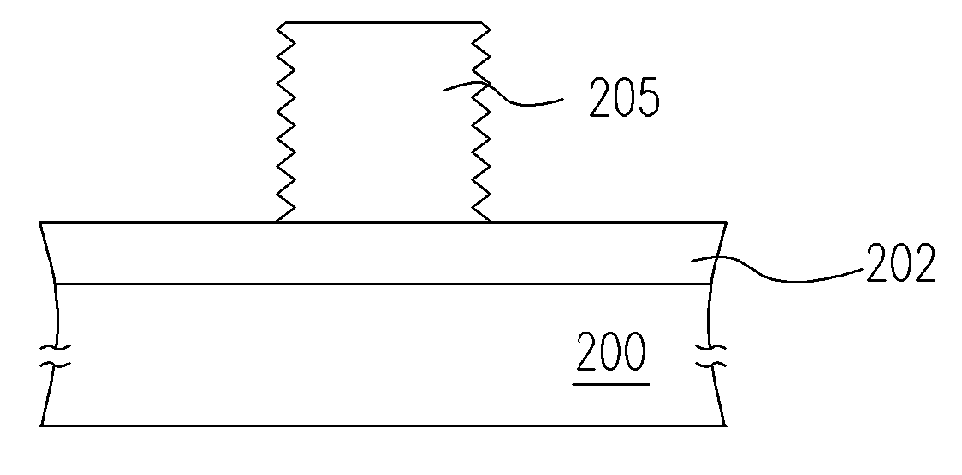
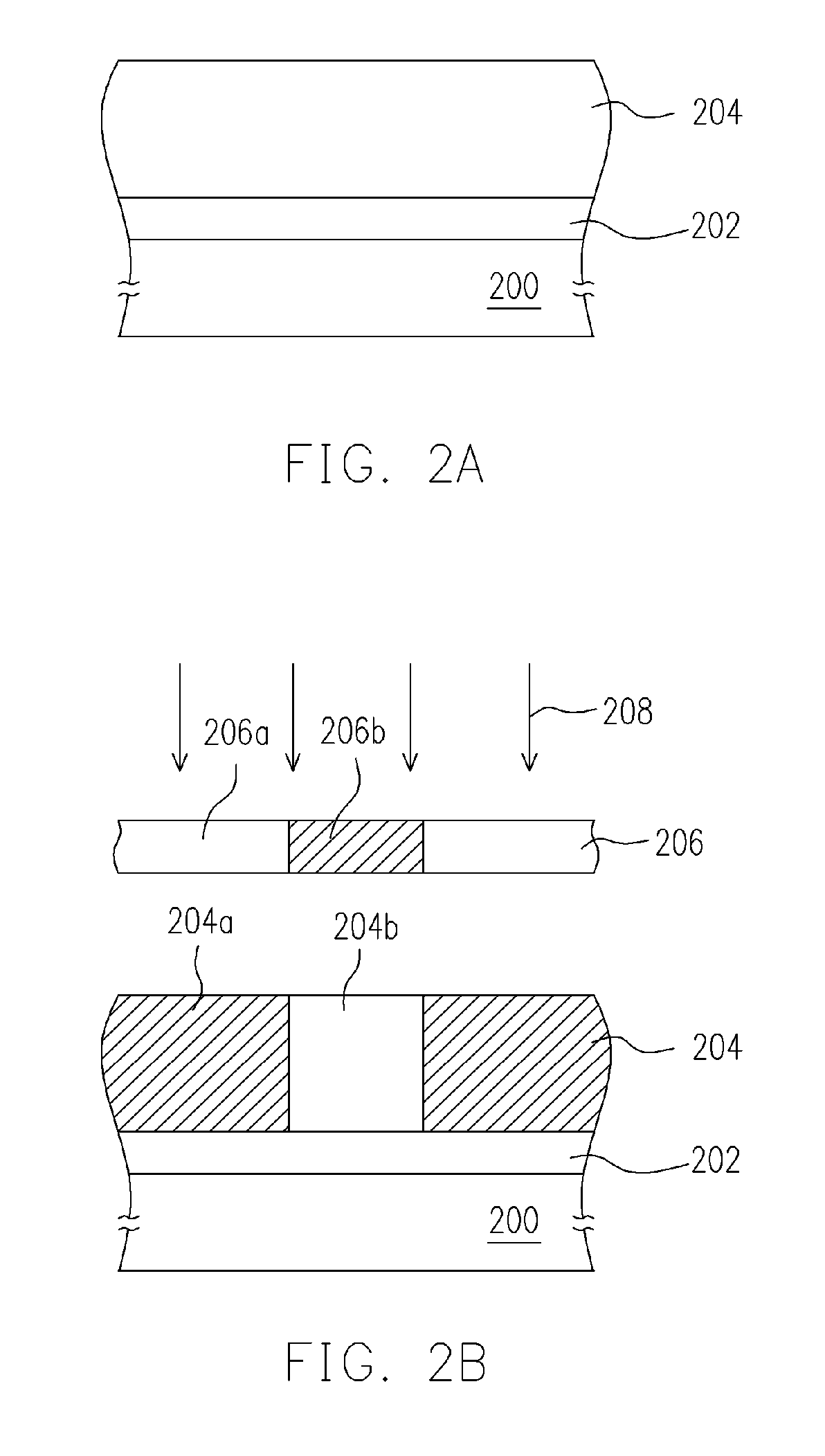
[0021] A method for forming a photoresist pattern including a method for trimming a pattern of a patterned photoresist layer according to this invention is shown in FIGS. 2A to 2D. Referring to 2A, a material layer 202 is formed over the substrate 200, while the material layer 202 can be a conductive or non-conductive layer. Wherein, the conductive layer is made of, for example, metal or polycrystalline silicon, while the non-conductive layer is made of, for example, silicon nitride, silicon oxide, or other dielectric material. A photoresist layer 204 is then formed over the material layer 202, wherein the photoresist layer 204 is made of, for example, a sensitive material as a mixture of a resin, sensitizer and solvent. The photoresist layer 204 is formed via a process including the steps of, for example, performing spin coating the sensitive material on the material layer 202, and then performing soft baking to remove the solvent in the sensitive material and to make the sensitive...


PUM

PropertyMeasurementUnit
pHaaaaaaaaaa
sizesaaaaaaaaaa
energyaaaaaaaaaa

Abstract

A method for forming a photoresist pattern is described. A photoresist layer is first formed over a substrate, and then an exposure process and a development process are performed to pattern the photoresist layer so as to form a patterned photoresist layer. Next, a multiple-trimming process is performed to trim the patterned photoresist lay to form a photoresist pattern. The multiple-trimming process includes at least one step of alkaline solution treatment and / or at least one step of neutral solution treatment. The method is applicable for improving properties of smoothness of the surface, and uniformity and minification of critical dimensions of the photoresist patterns.

Description

CROSS-REFERENCE TO RELATED APPLICATION [0001] This application claims the priority benefit of Taiwan application serial no. 93138539, filed on Dec. 13, 2004. All disclosure of the Taiwan application is incorporated herein by reference. BACKGROUND OF THE INVENTION [0002] 1. Field of the Invention [0003] The present invention generally relates to a photolithographic process, and more particularly to a method of forming a photoresist pattern and a method of trimming a photoresist pattern. [0004] 2. Description of the Related Art [0005] When the extent of integration of integrated circuits in electronic devices becomes ever-increased, the sizes of the entire electronic devices are getting smaller. Photolithography is an essential step during fabricating processes of semiconductor devices. In metal-oxide-semiconductor (MOS) devices, for instance, structural elements, such as patterns of various layers and regions with dopants, are all defined through a photolithographic process. The phot...

Claims


Application Information

Patent Timeline
Patent Type & Authority Applications(United States)
IPC IPC(8): G03F7/00
CPCG03F7/40
Inventor WU, CALVINCHANG, SHENG-YUEHHWANG, JAY
Owner UNITED MICROELECTRONICS CORP
Why Eureka
Try Eureka