Technique and methodology to passivate inductively coupled surface currents

a surface current and inductive coupling technology, applied in the field of integrated circuit inductors, can solve the problems of lessening the quality factor (q) of a device, reducing and affecting the quality of the device, so as to reduce the noise of the substrate and lessen the parasitic capacitance

Active Publication Date: 2006-06-15
BELL SEMICON LLC
View PDF3 Cites 8 Cited by
  • Summary
  • Abstract
  • Description
  • Claims
  • Application Information

AI Technical Summary

Benefits of technology

[0006] The present invention recognizes the disadvantages of the prior art and implants a deep n-well beneath the area of an inductor coil. The use of a deep n-well lessens the parasitic capacitance by placing a diode in series with the interlayer dielectric cap. The deep n-well also reduces substrate noise. Once the n-well is implanted and annealed, a cross hatch of shallow trench isolation is patterned over the n-well. The shallow trench isolation reduces and confines the inductively coupled surface currents to small areas that are then isolated from the rest of the chip.

Problems solved by technology

Such currents lessen the quality factor (Q) for a device and can cause latch-up and other failures on a chip.
If surface currents caused by an inductor are detrimental to an IC device, then the “Q” will be unacceptable.
SOI is an expensive process and, thus, may be considered disadvantageous for that reason alone.

Method used


Image

  • Technique and methodology to passivate inductively coupled surface currents
  • Technique and methodology to passivate inductively coupled surface currents
  • Technique and methodology to passivate inductively coupled surface currents

Examples


Embodiment Construction

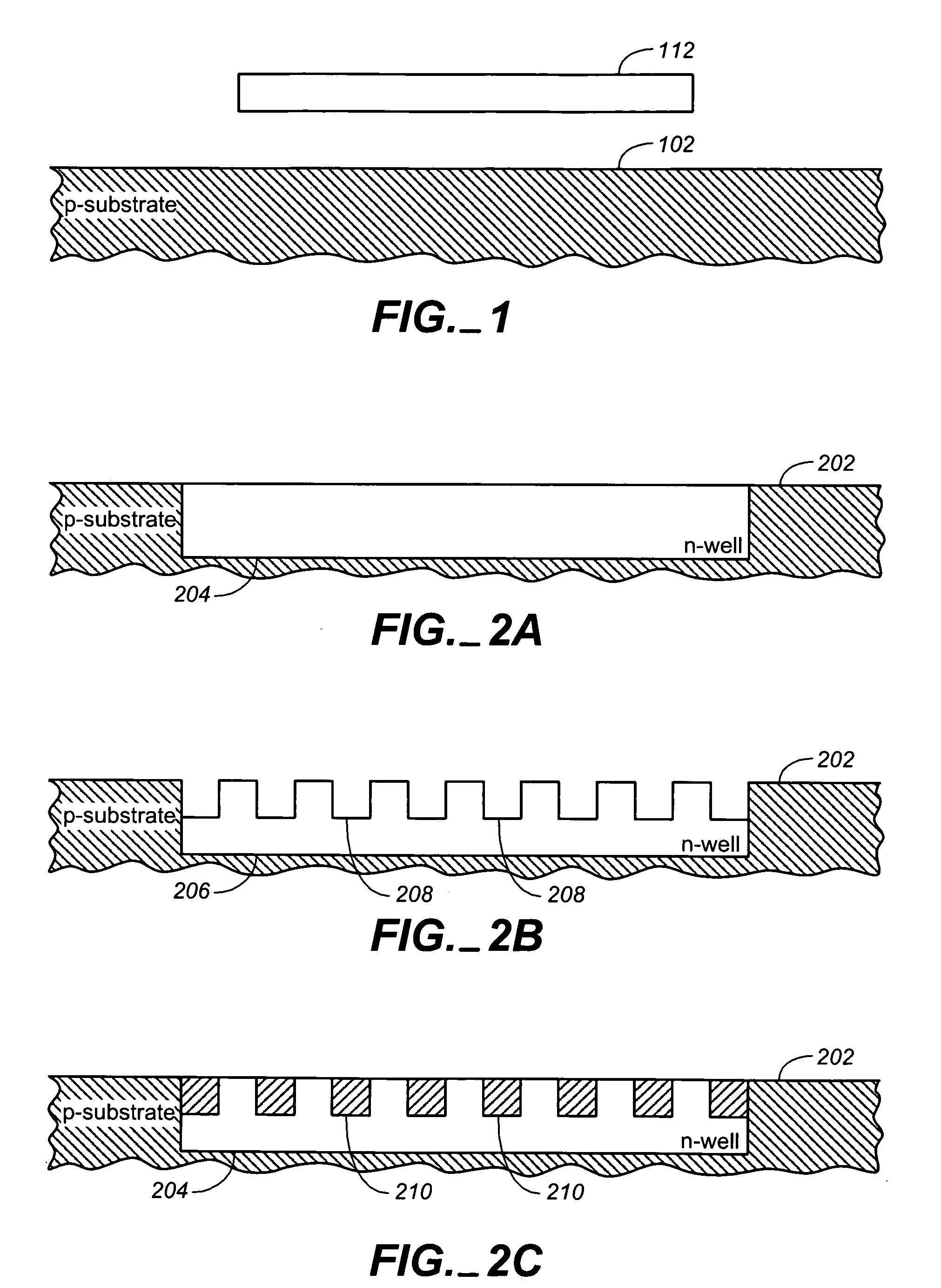
[0012] With reference now to the figures, FIG. 1 illustrates an IC inductor in accordance with an exemplary embodiment of the present invention. Inductor coil 112 is formed over p-substrate 102. Substrate 102 may have formed therein or thereon other components not shown. Substrate 102 is a lightly p-doped semiconductor. IC inductor 112 may cause inductively coupled surface currents on substrate 102. Such currents lessen the quality factor (Q) for a device and can cause latch-up and other failures on a chip.

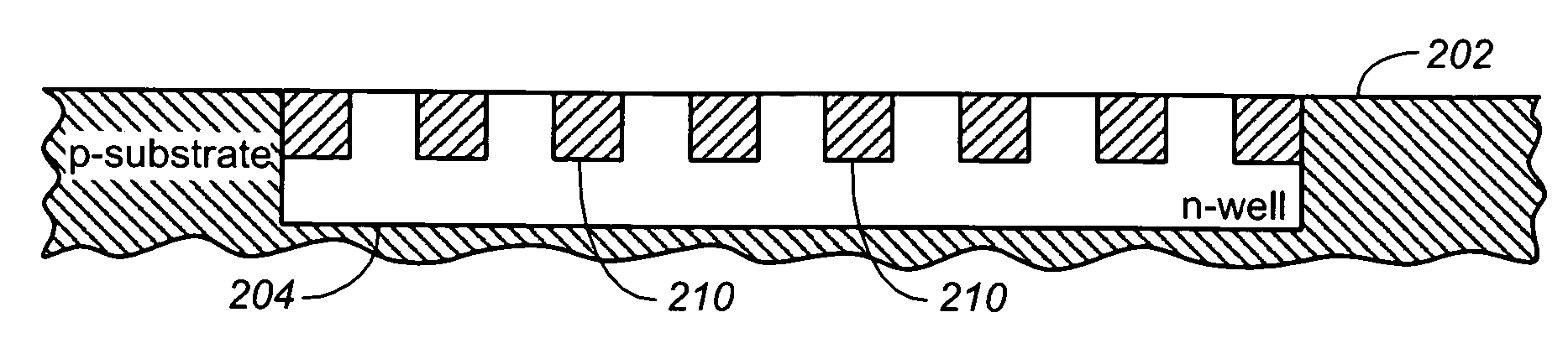
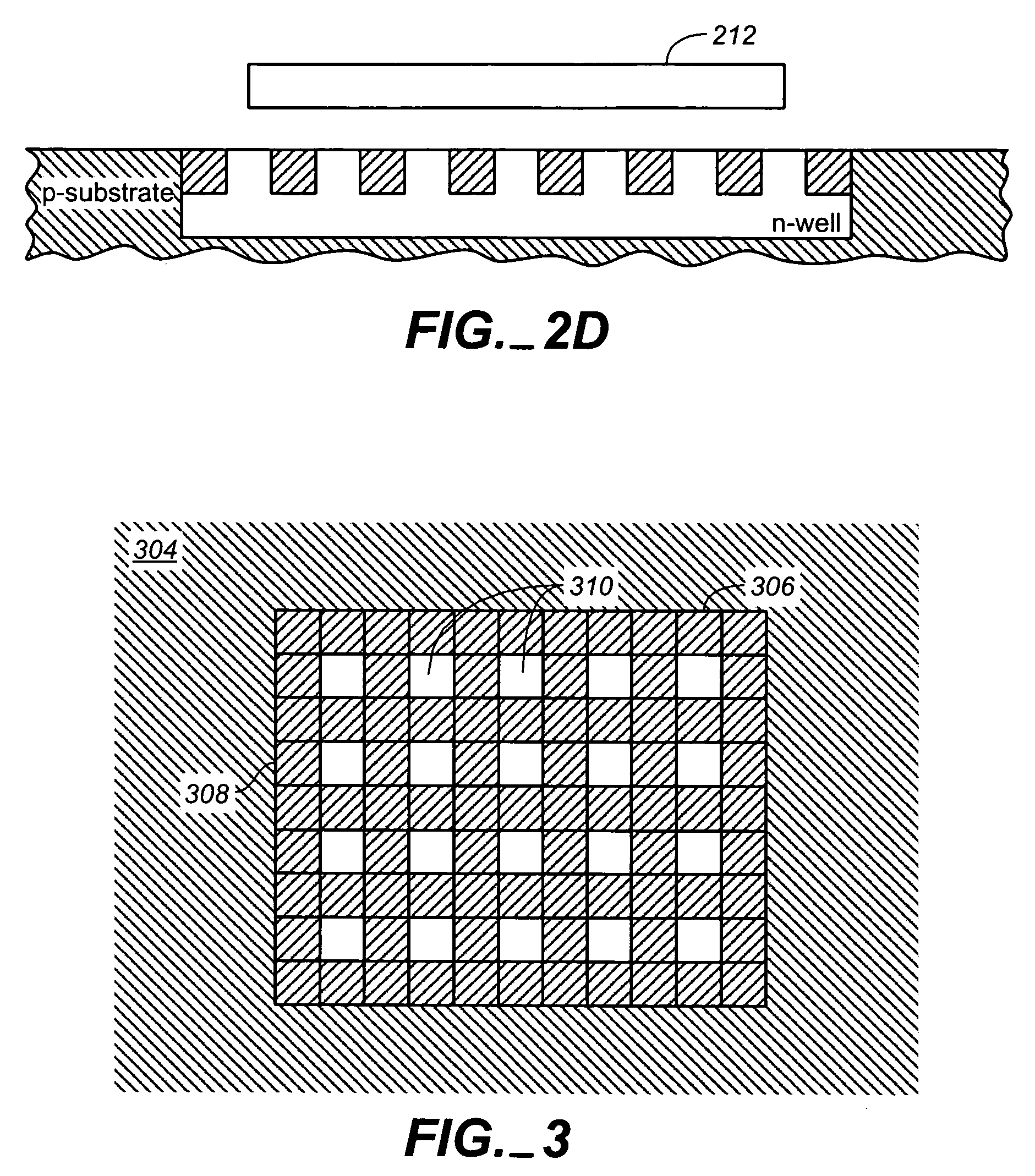
[0013]FIGS. 2A-2D depict the fabrication of a semiconductor device with an inductor coil in accordance with an exemplary embodiment of the present invention. More particularly, with reference to FIG. 2A, a deep n-well 204 is implanted into substrate 202. N-well 204 may be implanted through a window in a photoresist mask, for example. The n-well may be formed by a high-energy implant, typically phosphorus as the dopant. The implant dosage is typically on the order of 1×10¹⁶ atoms / ...


PUM


Abstract

A deep n-well is formed beneath the area of an inductor coil. The use of a deep n-well lessens the parasitic capacitance by placing a diode in series with the interlayer dielectric cap. The deep n-well also reduces substrate noise. Once the n-well is implanted and annealed, a cross hatch of shallow trench isolation is patterned over the n-well. The shallow trench isolation reduces and confines the inductively coupled surface currents to small areas that are then isolated from the rest of the chip.

Description

BACKGROUND OF THE INVENTION [0001] 1. Technical Field [0002] The present invention is directed generally toward integrated circuit inductors. More particularly, the present invention relates to a method and apparatus for passivating inductively coupled surface currents. [0003] 2. Description of the Related Art [0004] Integrated circuit (IC) inductors are inductive coils that are formed above a semiconductor device. IC inductors cause concern with inductively coupled substrate surface currents. Such currents lessen the quality factor (Q) for a device and can cause latch-up and other failures on a chip. The “Q” of a device, in this case, is a measure of how good the inductor is. If surface currents caused by an inductor are detrimental to an IC device, then the “Q” will be unacceptable. [0005] One solution to inductively coupled surface currents is to include floating poly and metal sheets underneath the inductor. The results of floating metal / poly sheets are unknown at this time. Ano...

Claims


Application Information

Patent Timeline
Patent Type & Authority Applications(United States)
IPC IPC(8): H01L21/76
CPCH01L21/76224H01L27/08
Inventor ERICKSON, SEAN CHRISTOPHERHUDSON, JASON DEE
Owner BELL SEMICON LLC
Why Eureka
Try Eureka