Back-contact photovoltaic cells
a photovoltaic cell and back-contact technology, applied in the field of new photovoltaic cells, can solve the problems of increasing the amount of time needed for photovoltaic cell manufacturing, consuming energy, and using high temperatures
- Summary
- Abstract
- Description
- Claims
- Application Information
AI Technical Summary
Benefits of technology
Problems solved by technology
Method used
Image
Examples
Embodiment Construction
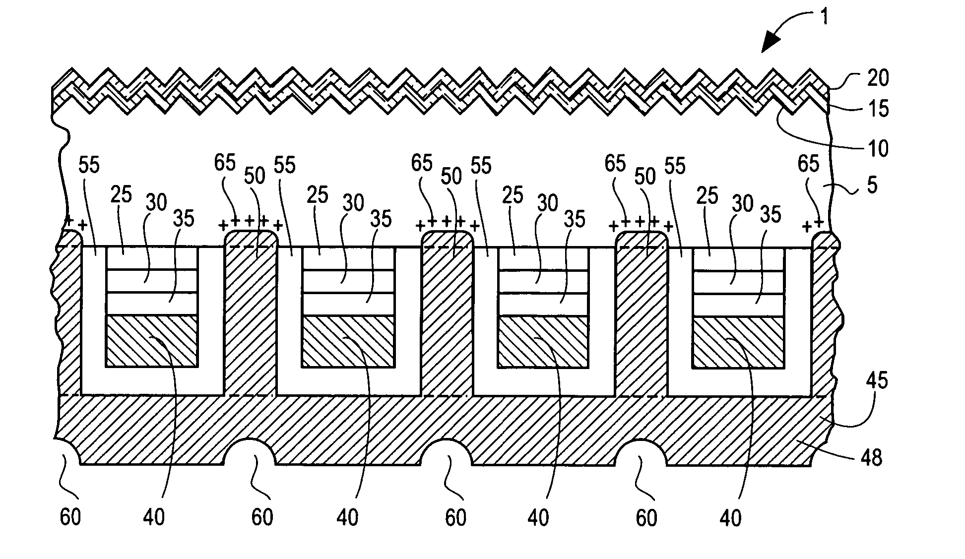
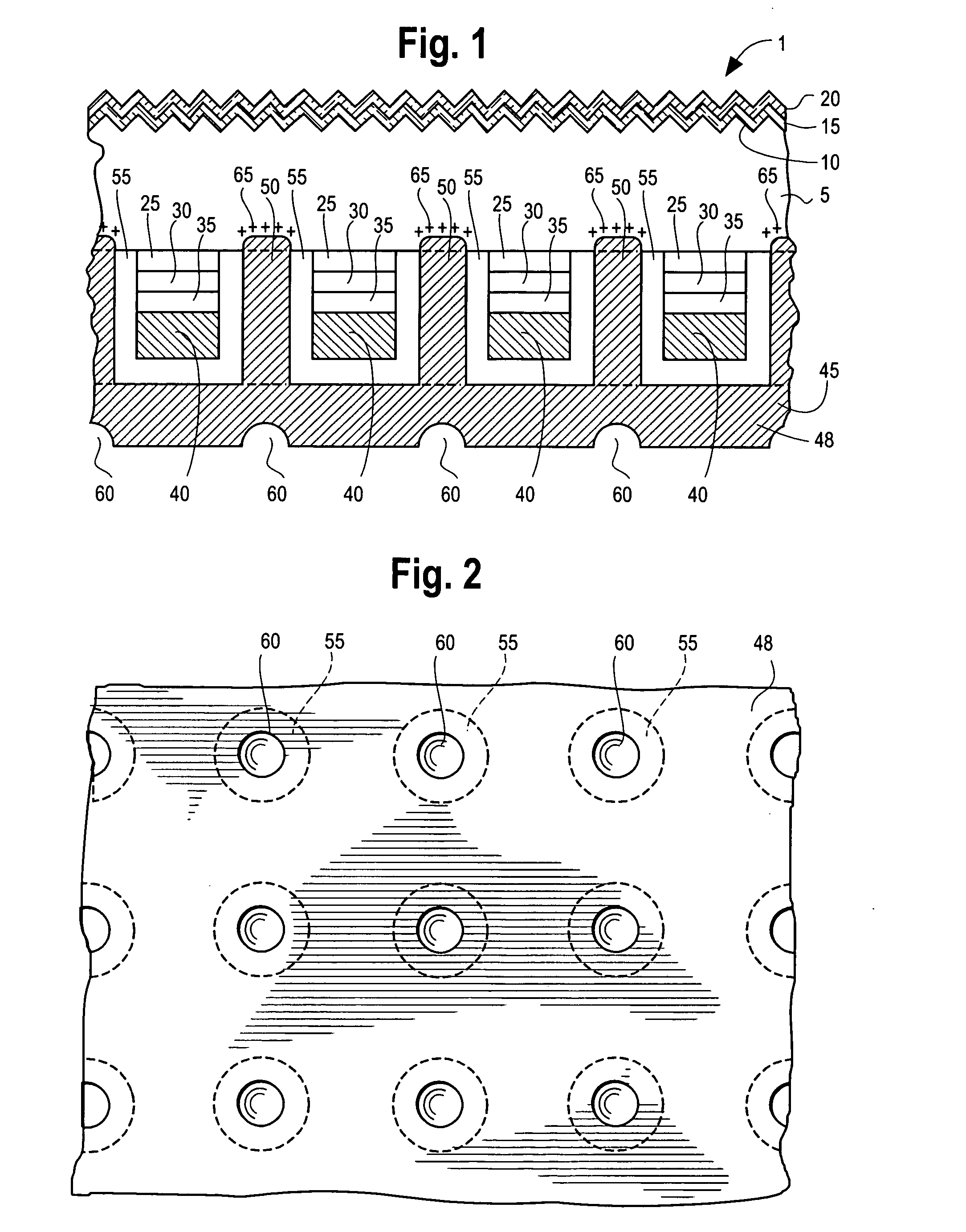
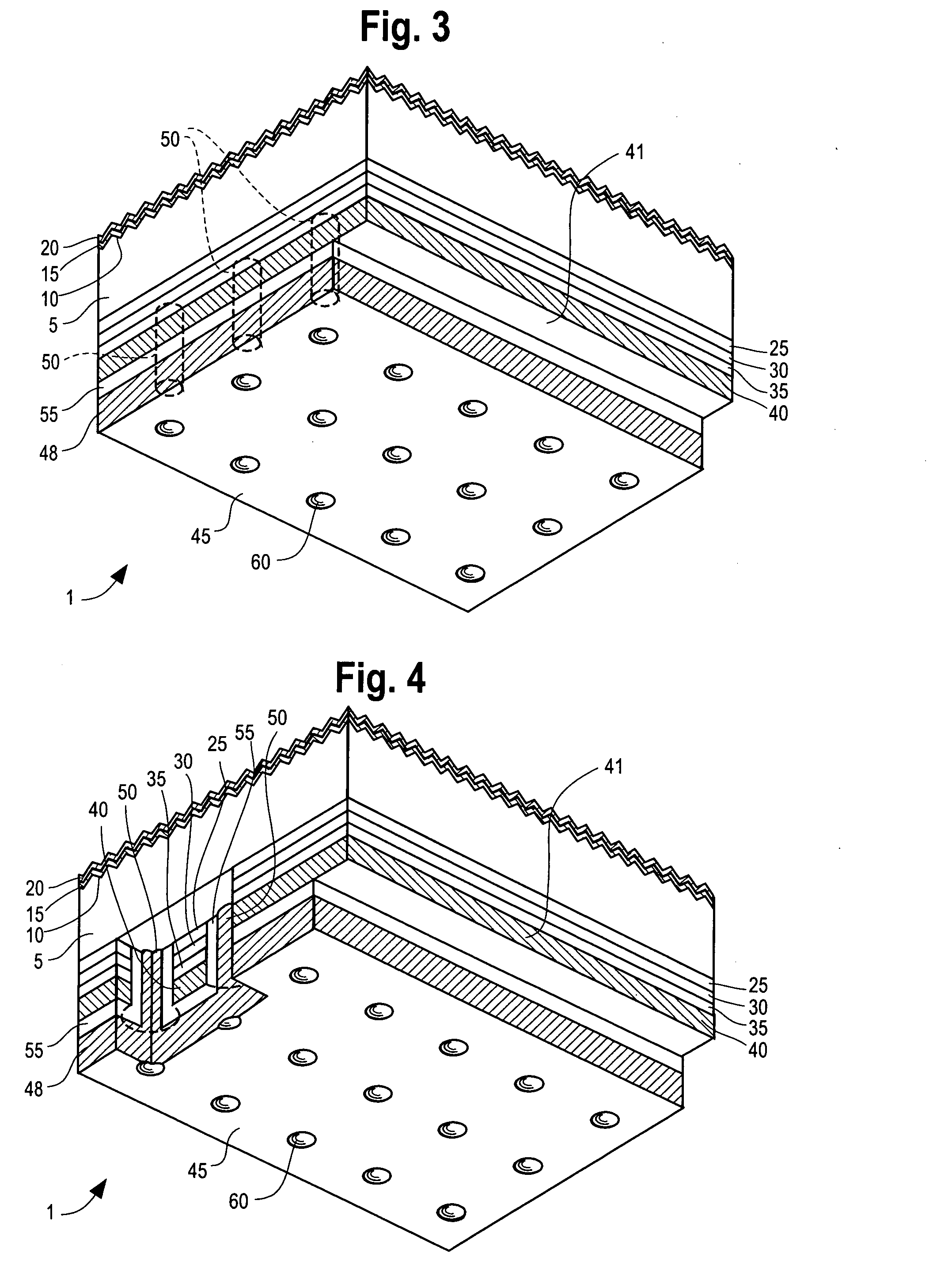
[0023] The invention will now be described using, as an example, an embodiment of the invention whereby a photovoltaic cell is made using a p-type, crystalline silicon wafer. However, it is to be understood that the invention is not limited thereby and is, for example, applicable to other semiconductor materials such as an n-type crystalline silicon wafer. In addition, it is not necessary for the wafer to be crystalline. It can, for example, be multi-crystalline or sometimes referred to as polycrystalline.
[0024] A silicon wafer useful in the process of this invention for preparing photovoltaic cells is typically in the form of a thin, flat shape. The silicon may comprise one or more additional materials, such as one or more semiconductor materials, for example germanium, if desired. Although boron is widely used as the first, p-type dopant, other p-type dopants, for example, aluminum, gallium or indium, will also suffice. Boron is the preferred p-type dopant. Combinations of such d...
PUM
 Abstract
Description
Claims
Application Information


