Method for controlling the spectral response of light sensitive elements, and image sensor with a controllable spectral response

a technology of light sensitive elements and controllable spectral response, which is applied in the field of image sensors, can solve the problems of poor color separation obtained in this fashion, high cost, and potential prone to long-term misalignment and ultimately image degradation

Active Publication Date: 2006-06-22
SAMSUNG ELECTRONICS CO LTD
View PDF21 Cites 34 Cited by
  • Summary
  • Abstract
  • Description
  • Claims
  • Application Information

AI Technical Summary

Benefits of technology

[0014] a circuit for applying a control voltage to said semiconductor element so as to change its spectral response.
[0015] Advantageous the light sensitive semiconductor element is a single photon avalanche diode operating In Geiger mode and said control signal being applied as a reverse bias voltage of said avalanche diode. The light sensitive semiconductor element comprises a multiplication region, and the thickness of said multiplication region is controlled with said control signal.

Problems solved by technology

The color separation obtained in this fashion is Imperfect due to the finite overlap of the various filters.
Another disadvantage is the fact that interpolation is always needed and that the useful size of a pixel is quadrupled, thus causing an effective reduction of lateral resolution.
This method is effective but expensive and potentially prone to long-term misalignment and ultimately image degradation.
The main disadvantage is however the need for moving parts that need be synchronized with the sensor's shutter, thus limiting the speed of the apparatus and, ultimately, its frame rate.
The main disadvantage of this method is a relatively shallow spectral response with a dull discrimination between the colors. FIG. 5 shows an example of the spectral response of the imager.
It may also cause a worsening of the signal to noise ratio in the image.
Indeed the noise may be significantly amplified by the procedure thus contributing to the degradation of the picture.

Method used


Image

  • Method for controlling the spectral response of light sensitive elements, and image sensor with a controllable spectral response
  • Method for controlling the spectral response of light sensitive elements, and image sensor with a controllable spectral response
  • Method for controlling the spectral response of light sensitive elements, and image sensor with a controllable spectral response

Examples


Embodiment Construction

[0032] In a preferred embodiment, the spectral response is changed by modulating the depth of the sensitive area of the light sensitive elements, using an appropriate control signal. Depth modulation enables capturing photons of different wavelengths at various rates.

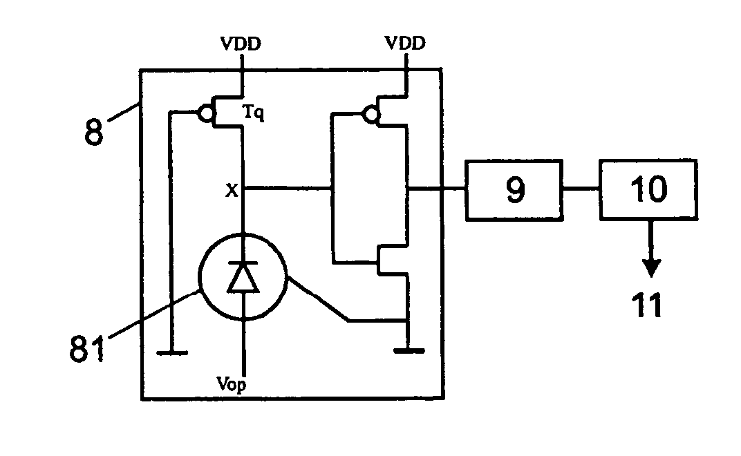
[0033] In a preferred embodiment, the light sensitive elements are based on the Single Photon Avalanche Diode (SPAD) technology. SPADs are optical detectors sensitive to the arrival of a single photon. They are also known as photon counting devices. A SPAD operating in Geiger mode is a diode 81, or p-n junction, that is reverse biased beyond its breakdown voltage. Under those conditions the diode 81 p-n junction may trigger an avalanche upon photon arrival. Such zone is called multiplication region 5. FIG. 6 shows a cross-section example of a SPAD implemented In CMOS technology. Other structures are also possible in the framework of the invention and have been successfully demonstrated. The multiplication region 5, a g...


PUM


Abstract

It is disclosed a method for controlling the spectral response of light sensitive semiconductor elements in an array (8) using an electric control signal (Vop) applied to said semiconductor elements. The light sensitive semiconductor elements could be a single photon avalanche diode (81) operating In Geiger mode. The invention as well refers to an Image sensor comprising at least one light sensitive semiconductor elements and a circuit for applying a control voltage (Vop) to said semiconductor element so as to change its spectral response. Without being limiting, the sensor of the invention could be part of a digital camera, video camera, 3D image sensors, scanner, video telephone, autofocus system, medical image acquisition system, etc.

Description

FIELD OF INVENTION [0001] The present invention relates to image sensors, in particular to color image sensor for 2D or 3D image acquisition. In particular the present invention relates to a method for controlling the spectral response of light sensitive semiconductor elements in an array according to the independent claim 1 and to an image sensor with the characteristics according to the Independent claim 15. STATE OF THE ART [0002] Conventional imagers can detect colored scenes by reconstructing a mosaic of pixels mostly sensitive to one of the primary colors (red “R”, green “G”, and blue “B”). Pixels are made selectively sensitive by covering them with a color filter. The filtering pattern is usually repeated over a matrix of 2×2 pixels favoring green. FIG. 1 shows one such color pattern as it is implemented in conventional solid-state imagers. [0003] The separation of colors is dependent of the selectivity of the three filters. The spectral response |H| measured in typical filte...

Claims


Application Information

Patent Timeline
Patent Type & Authority Applications(United States)
IPC IPC(8): H01J40/14H01L31/00
CPCG01J1/0488G01J1/44H01L27/14645H01L31/101H01L31/107H04N3/155H04N25/772
Inventor CHARBON, EDOARDONICLASS, CRISTIANO
Owner SAMSUNG ELECTRONICS CO LTD
Why Eureka
Try Eureka