Semiconductor device and method of fabricating the same

a semiconductor and electrode technology, applied in the direction of semiconductor devices, semiconductor/solid-state device details, electrical apparatus, etc., can solve the problems of deterioration of the solder-wetting property of the anode electrode, difficulty in thinning the device, and difficulty in ensuring a high current-proof.

Inactive Publication Date: 2006-06-22
KK TOSHIBA
View PDF8 Cites 23 Cited by
  • Summary
  • Abstract
  • Description
  • Claims
  • Application Information

AI Technical Summary

Problems solved by technology

The above-described high-voltage semiconductor device with the conventional wire-bonding scheme has drawbacks such as: it is difficult to thin the device due to the bonding wire; and it is difficult to secure a high current-proof.
However, when such the solder-bonding scheme is adapted to a planer-type semiconductor device, another problem occurs.
If the passivation process is performed in a high temperature circumstance of about 300° C. or more after having formed the anode electrode, it will be generated melting of Ni, oxidization of Au and the like, and thereby resulting in that the solder-wetting property of the anode electrode is deteriorated.
As a result, the mode of the depletion layer extending at a reverse bias application time may become different from a desirable state, and the breakdown voltage property will be deteriorated.
This will lead to insulation breakdown and deterioration of the device characteristics.
As described above, there are various problems in the double-sided solder-bonding scheme for planar-type semiconductor devices.

Method used


Image

  • Semiconductor device and method of fabricating the same
  • Semiconductor device and method of fabricating the same
  • Semiconductor device and method of fabricating the same

Examples


Embodiment Construction

[0034] Illustrative embodiments of this invention will be explained with reference to the accompanying drawings below.

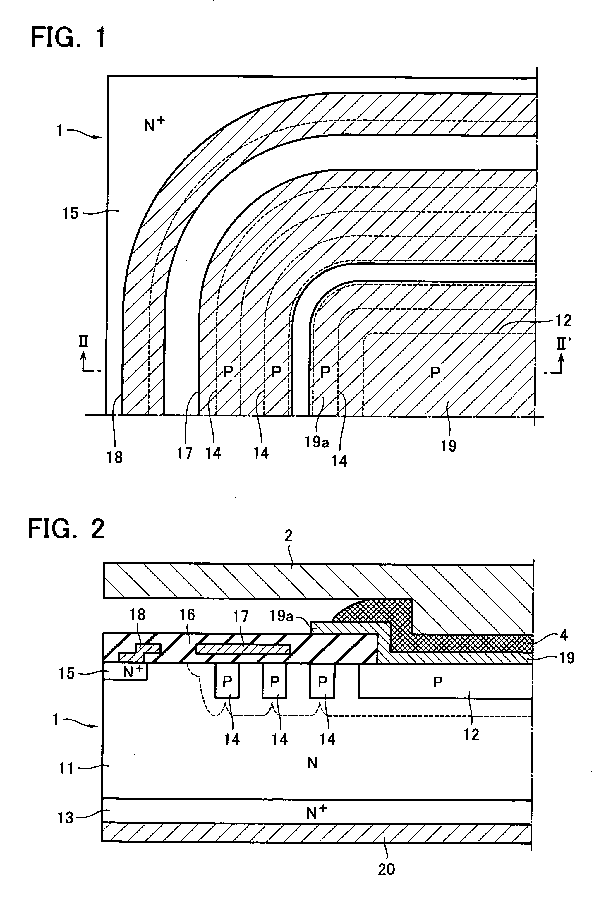
[0035]FIG. 6 is a plan view of a semiconductor device in accordance with an embodiment, and FIGS. 7 and 8 are sectional views of the device taken along line I-I′ in FIG. 6, respectively. The semiconductor device chip 1 is a high-breakdown planer-type one, upper and lower terminal electrodes of which are bonded to upper and lower conductive frames formed of, for example, Cu, with solder material 4. The device chip 1 and frames 2 and 3 are sealed with resin mold 5.

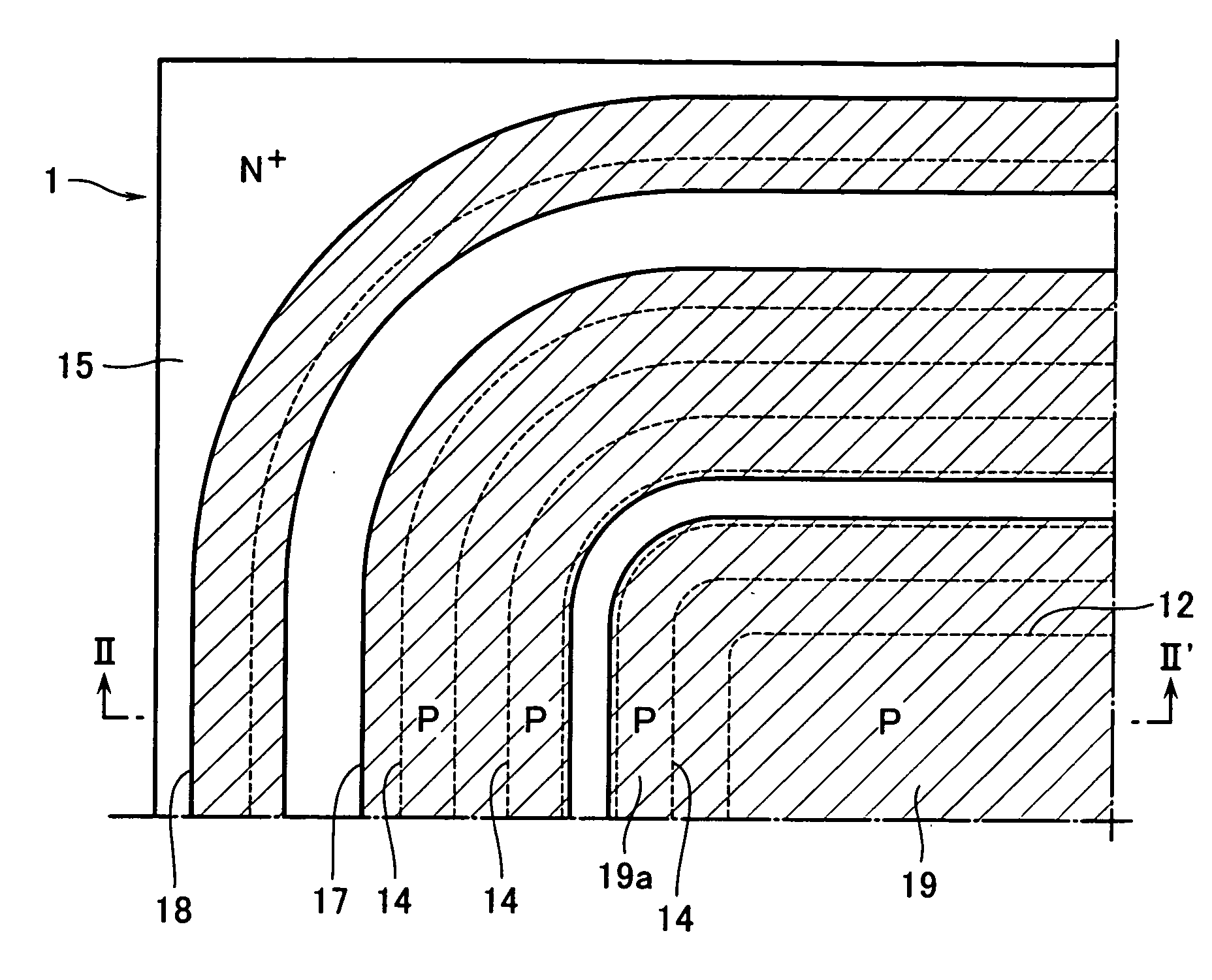
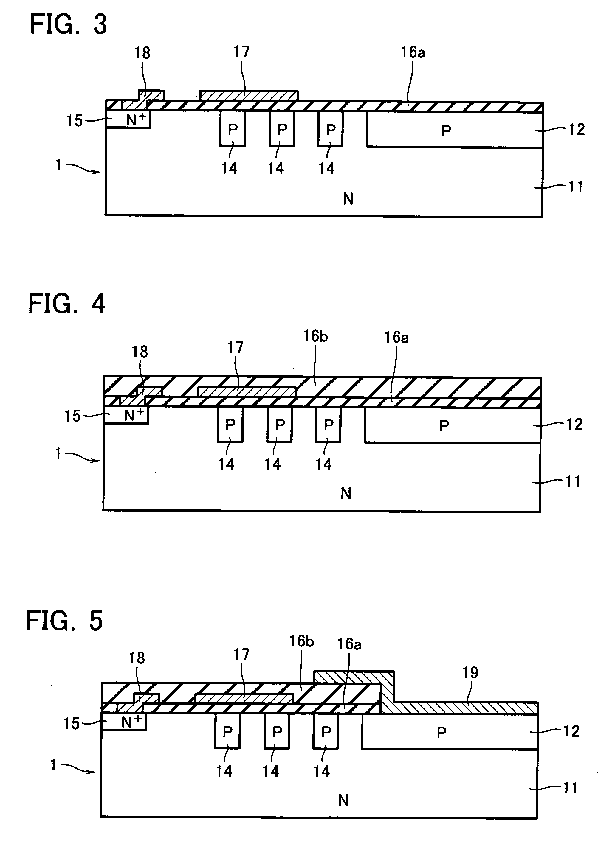
[0036]FIG. 1 is a plan view of the quartered semiconductor device chip 1, and FIG. 2 is a sectional view of the device taken along line II-II′ in FIG. 1. The semiconductor device chip 1 is a rectify-use PN junction diode with a high resistive N-type semiconductor substrate 11 serving as a base semiconductor layer. A P-type diffusion layer serving as an anode layer 12 is selectively formed in the top surface...


PUM


Abstract

A semiconductor device has a semiconductor device chip with upper and lower terminal electrodes, and upper and lower frames bonded to the upper and lower terminal electrodes, respectively, with solder material, wherein the semiconductor device chip includes: a semiconductor layer of a first conductivity type; a diffusion layer of a second conductivity type, which is selectively formed in the semiconductor layer; a plurality of guard-ring layers of the second conductivity type, which are formed outside of the diffusion layer in the semiconductor layer; an insulating film formed on the semiconductor layer; and a field plate formed of a poly-crystalline silicon film embedded in the insulating film.

Description

CROSS-REFERENCE TO RELATED APPLICATION [0001] This application is based on and claims the benefit of priority from the prior Japanese Patent Application No. 2004-365655, filed on Dec. 17, 2004, the entire contents of which are incorporated herein by reference. BACKGROUND OF THE INVENTION [0002] 1. Field of the Invention [0003] This invention relates to a semiconductor device with a guard-ring structure for achieving a high breakdown voltage property and a method of fabricating the device. More specifically, the invention relates to a semiconductor device, in which upper and lower electrodes of a planer-type device chip are bonded to upper and lower conductive frames respectively with solder material. [0004] 2. Description of Related Art [0005] In the field of power-use semiconductor devices, there has been provided such a technique that guard-ring layers are formed to surround a terminal diffusion layer, and a field plate is disposed above the guard-ring layers for controlling the d...

Claims


Application Information

Patent Timeline
Patent Type & Authority Applications(United States)
IPC IPC(8): H01L29/47H01L21/28
CPCH01L23/488H01L23/49562H01L2924/1305H01L2924/13091H01L2224/05552H01L2224/05572H01L2224/33181H01L2224/26145H01L2224/291H01L2224/27013H01L2924/0002H01L2924/01023H01L2924/01006H01L2924/00014H01L2224/32245H01L2924/3011H01L2924/05042H01L2924/014H01L2924/01082H01L24/03H01L24/05H01L24/33H01L24/48H01L29/0619H01L29/0638H01L29/402H01L29/8611H01L2224/02166H01L2224/04042H01L2224/05556H01L2224/05624H01L2224/48095H01L2224/48463H01L2924/01004H01L2924/01005H01L2924/01013H01L2924/01014H01L2924/01015H01L2924/01022H01L2924/01027H01L2924/01028H01L2924/01029H01L2924/01033H01L2924/01047H01L2924/01079H01L2224/45099H01L2924/00H01L2924/12036H01L2924/12041H01L2924/181H01L2924/00012
Inventor WATANABE, MITSURUFUKUI, TETSUYA
Owner KK TOSHIBA
Why Eureka
Try Eureka