Display element stress free at the critical layer

a technology of stress-free and critical layer, applied in the field of flexible organic lightemitting diodes (oled) and liquid crystal displays, can solve the problems of changing the thickness of the crystal layer, affecting the natural flexibility of the plastic substrate, and affecting the display effect, so as to avoid stress-induced damage and failure of the display

Inactive Publication Date: 2006-06-22
EASTMAN KODAK CO
View PDF8 Cites 34 Cited by
  • Summary
  • Abstract
  • Description
  • Claims
  • Application Information

AI Technical Summary

Benefits of technology

[0016] The invention provides a display device, and more particularly a flexible display device that remains substantially flat and the stress in at least one layer of the light-emitting module in the display is substantially zero throughout the operating temperatures. It is important for the display to remain flat for better viewing. Furthermore, since the stress in one layer of the light-emitting module is substantially zero throughout the operating temperature range, this layer can be chosen to be the most vulnerable layer in the light-emitting module to avoid stress-induced damage and failure of the display due to temperature changes.

Problems solved by technology

On the other hands, under bending moments, the rigid display tends to lose its image over a large area, due to the fact that the gap between the substrates changes, thereby causing the liquid crystal and OLED materials to flow away from the bending area, resulting in a changed crystal layer thickness.
Consequently, displays utilizing glass substrates are less suitable, when a more flexible or even bendable display is desired.
However, the natural flexibility of the plastic substrates presents problems, when trying to manufacture liquid crystal displays in a traditional manner.
The flexibility of the display is limited by the bending limitation of the display enclosures.
However, the introduction of grooves to the substrate causes significant stress concentration in the grooves.
This may lead to substrate fracture during manufacturing or usage.
When these structures carry an electrical current, joule heating takes place, and there is a potential for deleterious structural stress due to the mismatch of thermal expansion coefficients from one layer to the next.
The prior art has attempted to address the aforementioned drawbacks and disadvantages, but has achieved mixed results.
This method is generally less than ideal, since it adds unnecessary thickness to a device that is required to be sufficiently thin.
Additionally, such thickness restrictions hinder the possibility of employing additional layers that may be needed to minimize thermal stress.
This method has a distinct disadvantage in that it does not provide flexibility in adjusting the coefficient of thermal expansion and the thickness of the respective layers.

Method used


Image

  • Display element stress free at the critical layer
  • Display element stress free at the critical layer
  • Display element stress free at the critical layer

Examples


Embodiment Construction

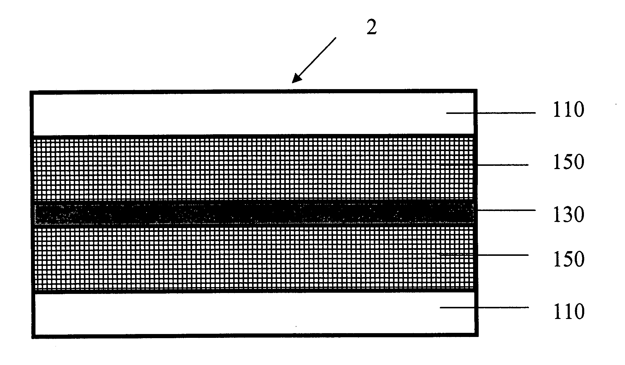
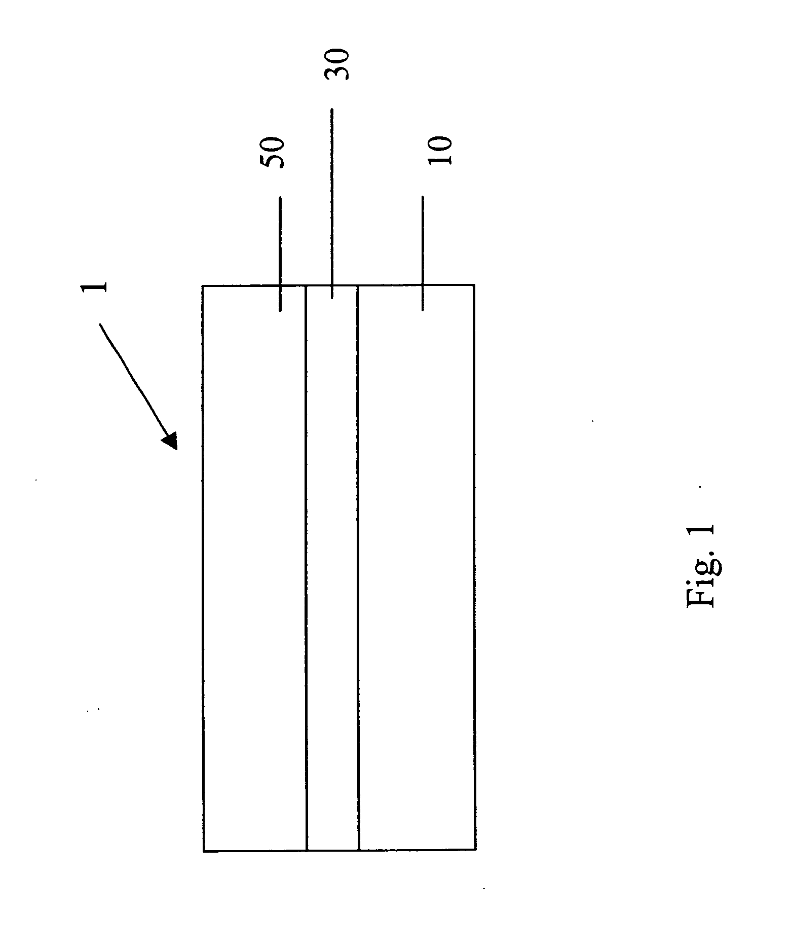
[0024] Referring to FIG. 1, embodiment 1 of the present invention consists of a substrate 10, a flexible light-emitting module 30 which includes light-emitting material, an anode, and a cathode (not shown), and a superstrate 50. These layers are described in detail below.

[0025] Note that the substrate may alternatively be located adjacent to the cathode, or the substrate may actually constitute the anode or cathode. The flexible light-emitting module may contain organic layers and other layers such as a hole-injecting layer, a hole-transporting layer, and electron-transporting layer. The total combined thickness of the organic layers is typically less than 500 nm as disclosed in U.S. Pat. No. 6,771,021.

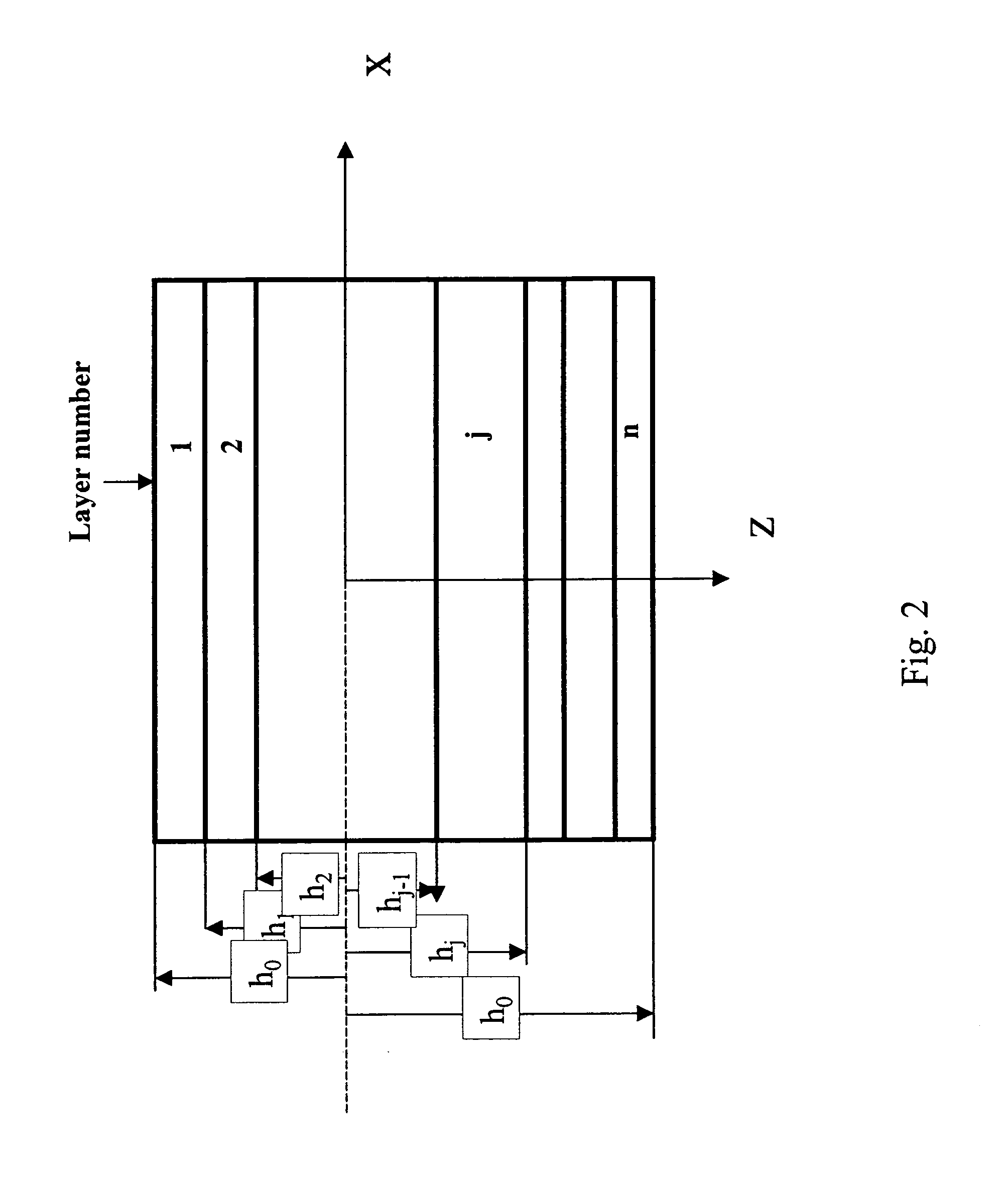
[0026] Flexible displays are made of multilayered thin films. These film layers have different thickness, thermal / moisture expansion coefficients and thermal shrinkage behavior that results in deflection and bending stress due to temperature changes. The deflection and stress can af...


PUM


Abstract

The invention relates to a display device, and more particularly a flexible display device comprising display component layers and display substrate such that the display remains substantially flat throughout the operating temperatures. The invention further relates a display device, and more particularly a flexible display device comprising display component layers and display substrate such that the stress in at least one layer of the light-emitting module in the display is substantially zero throughout the operating temperature range. These and other objects of the invention are accomplished by providing a flexible display, comprising at least one planar flexible substrate, at least one flexible light-emitting module deposited on the flexible substrate, the light-emitting module including at least one light-emitting layer, an anode, a cathode, and at least one top flexible superstrate on the opposite side of said display from said planar flexible substrate wherein the display is thermoelastically balanced in such a way that the display is always substantially flat, and the stress in at least one layer of the light-emitting module is substantially zero throughout the operating temperature range.

Description

FIELD OF THE INVENTION [0001] This invention relates in general to a display device, and more particularly to a flexible organic light-emitting diode (OLED) and liquid crystal displays (LCD) devices comprising properly selected layers so that the display remains flat, and the thermal stress in the display can be reduced to avoid failure. BACKGROUND OF THE INVENTION [0002] Most of commercial displays devices, for example, liquid crystal displays (LCD), or solid-state organic light-emitting diode (OLED) are rigid. LCD comprise two plane substrates, commonly fabricated by a rigid glass material, and a layer of a liquid crystal material or other imaging layer, and arranged in-between said substrates. The glass substrates are separated from each other by equally sized spacers being positioned between the substrates, thereby creating a more or less uniform gap between the substrates. Further, electrode means for creating an electric field over the liquid crystal material are provided and ...

Claims


Application Information

Patent Timeline
Patent Type & Authority Applications(United States)
IPC IPC(8): H05B33/02H05B33/00
CPCH01L51/5237H01L2251/5338H10K2102/311H10K59/87H10K50/84
Inventor GAO, ZHANJUNFURLANI, EDWARD P.
Owner EASTMAN KODAK CO
Why Eureka
Try Eureka