CMOS image sensors having pixel arrays with uniform light sensitivity

Active Publication Date: 2006-06-22
SAMSUNG ELECTRONICS CO LTD
View PDF12 Cites 87 Cited by
  • Summary
  • Abstract
  • Description
  • Claims
  • Application Information

AI Technical Summary

Benefits of technology

[0013] In general, exemplary embodiments of the invention include solid state CMOS active pixel sensor devices having improved response uniformity. More specifically, exemplary embodiments of the invention include methods for fabricating CMOS active pixel sensors having pixel arrays with unit pixels that are designed to provide increased uniformity of pixel-to-pixel sensitivity across the pixel array without the need for an additional light shielding layer. In one exemplary embodiment of the invent

Problems solved by technology

In contrast, CCD image sensor devices are expensive to fabricate, typically require 2, 3 or more supply voltages at different clock speeds with significantly higher power consumption, and do not allow random access to unit pixels.
Compared to solid state CCDs, however, conventional CMOS active pixel sensors have lower “fill factors”, which results in degraded performance (e.g., low sensitivity to incident light, low quantum efficiency, poor signal-to-noise ratio and limited dynamic range.).
Consequently, the generation of photo charges in the transistor region (22) can result in noise and cause non-uniform pixel response across the pixel array.
The use of additional light shields, however, result in reduced pixel fill factor and lower Quantum Efficiency (QE) performance (and

Method used


Image

  • CMOS image sensors having pixel arrays with uniform light sensitivity
  • CMOS image sensors having pixel arrays with uniform light sensitivity
  • CMOS image sensors having pixel arrays with uniform light sensitivity

Examples


Embodiment Construction

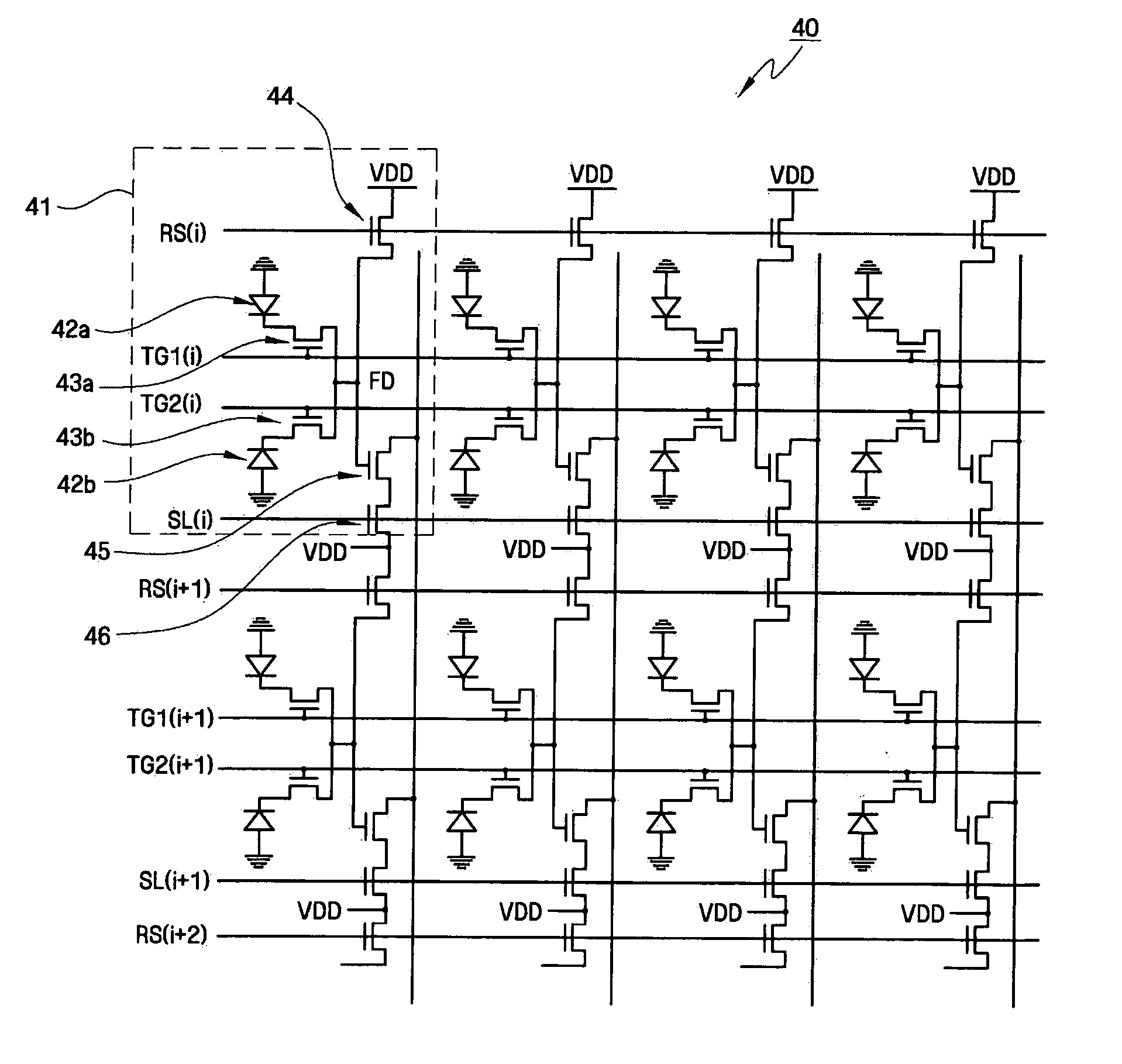
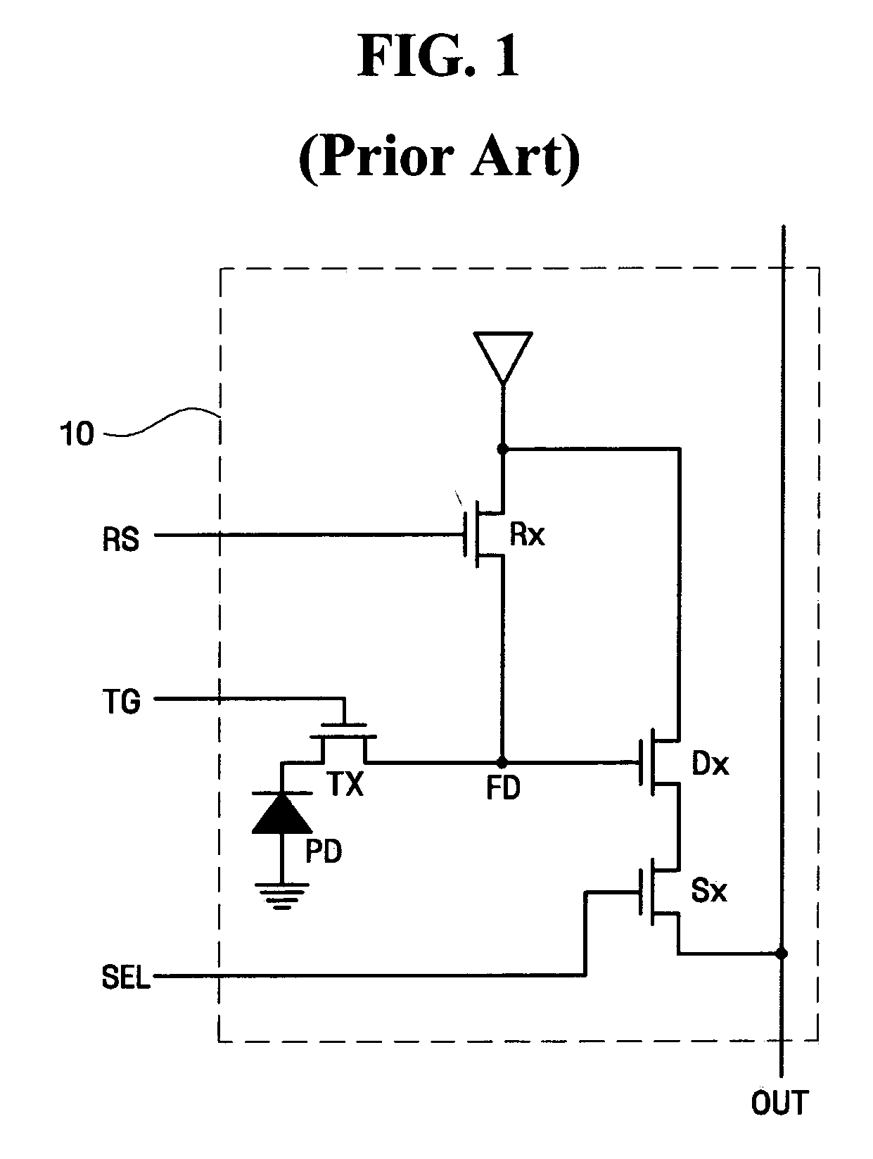
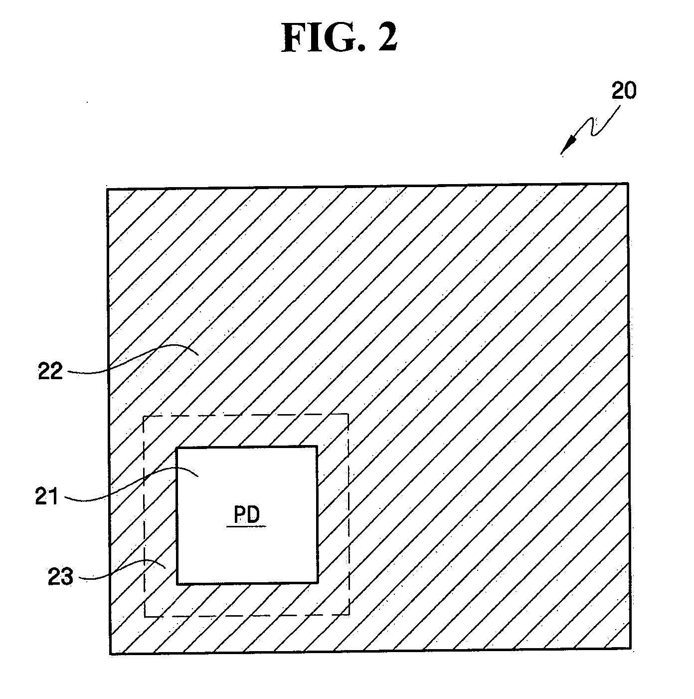
[0026] Exemplary embodiments of solid state CMOS active pixel sensor devices having improved response uniformity will now be discussed in further detail with reference to accompanying drawings. It is to be understood that the drawings are merely schematic depictions where the thickness and dimensions of various components, layers and regions are not to scale, but rather exaggerated for purposes of clarity. It is to be further understood that when a layer is described herein as being “on” or “over” another layer or substrate, such layer may be directly on the other layer or substrate, or intervening layers may also be present. It is to be further understood that the same reference numerals used throughout the drawings denote elements that are the same or similar or have the same or similar functions.

[0027] In general, exemplary embodiments of the invention as described herein include methods for fabricating CMOS active pixel sensors having pixel arrays in which the pixel structures ...


PUM


Abstract

Solid state CMOS active pixel sensor devices having unit pixels that are structured to provide improved uniformity of pixel-to-pixel sensitivity across a pixel array without the need for an additional light shielding layer. For example, unit pixels with symmetrical layout patterns are formed whereby one or more lower-level BEOL metallization layers are designed operate as light shielding layers which are symmetrically patterned and arranged to balance the amount of incident light reaching the photosensitive regions.

Description

CROSS-REFERENCE TO RELATED APPLICATION [0001] This application claims priority to Korean Patent Application No. 10-2004-0107181, filed on Dec. 16, 2004, which is fully incorporated herein by reference. TECHNICAL FIELD OF THE INVENTION [0002] The present invention relates generally to CMOS active pixel sensor devices having improved response uniformity and, in particular, methods for fabricating CMOS active pixel sensor devices having pixels structures that provide increased uniformity of pixel-to-pixel sensitivity across a pixel array. BACKGROUND [0003] Various types of solid state imaging devices / have been developed, which primarily include charge-coupled devices (CCDs) and complementary metal oxide semiconductor (CMOS) image sensor devices, as well as hybrid image sensors that are based on a combination of CCD and CMOS image sensor designs. In general, CCD and CMOS solid state imaging sensors CCD image sensors operate based on the “photoelectric effect”, which occurs when silicon ...

Claims


Application Information

Patent Timeline
IPC IPC(8): H04N5/335
CPCH01L27/14603H01L27/14623H01L27/14643H01L27/14689H01L27/146H01L21/28H04N25/76
Inventor NAM, JUNG HYUNLEE, YUN HEE
Owner SAMSUNG ELECTRONICS CO LTD
Why Eureka
Try Eureka