Method of manufacturing a semiconductor device

a manufacturing method and semiconductor technology, applied in the field of semiconductor device manufacturing, can solve the problems of reducing yield, affecting the efficiency of semiconductor devices, and difficult implanting of interlayer insulating layers, and achieve the effect of suppressing the fluctuation of the threshold voltage of transistor arrangement, without causing a decrease in yield

Inactive Publication Date: 2006-06-22
SHARP KK
View PDF5 Cites 1 Cited by
  • Summary
  • Abstract
  • Description
  • Claims
  • Application Information

AI Technical Summary

Benefits of technology

[0010] The present invention has been developed in view of the above problem. An object of the present invention is to provide a method of manufacturing a semiconductor device provided with memory cells of the floating gate type, where the silicon nitride layer is deposited on a control gate electrode as an etching stop layer for bottom borderless contact process while suppressing fluctuation in threshold voltage of transistor arrangement and without causing a decrease in yield.

Problems solved by technology

This causes the inter-layer insulating layer to be implanted with much difficulty when the etching stop layer for bottom borderless contact process, such as self-aligned contact arrangement, is deposited to a required thickness.
However, the deposition of a silicon nitride layer by the low pressure CVD technique has the following drawback.
This causes fluctuation in the threshold voltage of the transistor arrangement, and results in a decrease in yield.

Method used


Image

  • Method of manufacturing a semiconductor device
  • Method of manufacturing a semiconductor device
  • Method of manufacturing a semiconductor device

Examples


Embodiment Construction

[0024] A method of manufacturing a semiconductor device (hereinafter referred to as an inventive method) according to the present invention will be described in more detail referring to the relevant drawings. It is noted that the semiconductor device manufactured by the inventive method as one embodiment of the present invention is a nonvolatile semiconductor storage device (flash memory) composed of a matrix of flash memory cells. It would also be understood that the inventive method is not limited to the following description.

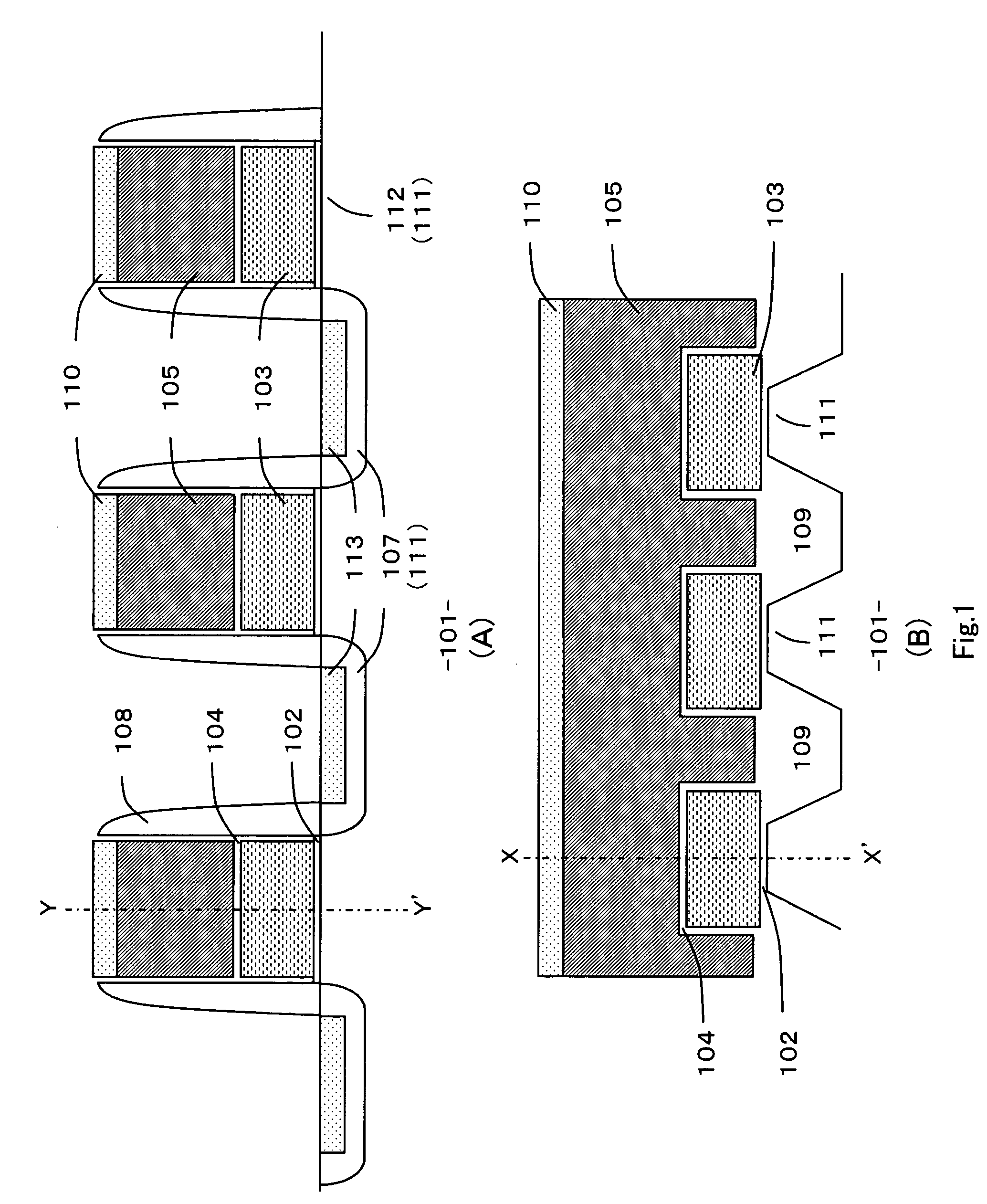
[0025] The description starts with a transistor structure of the memory cells and a relevant transistor structure of other peripheral circuits than the memory cells, referring to FIGS. 1 and 2.

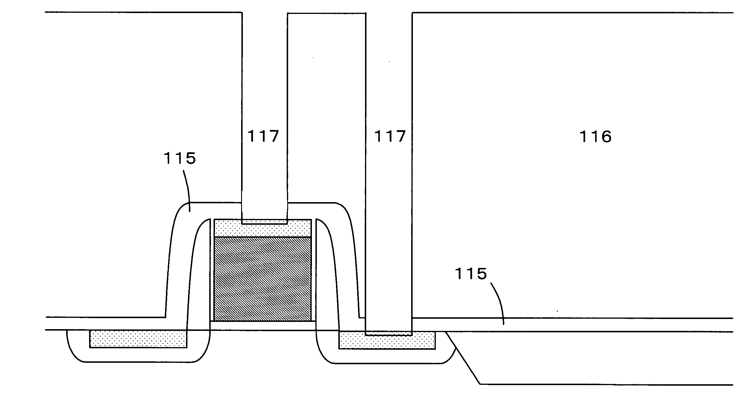
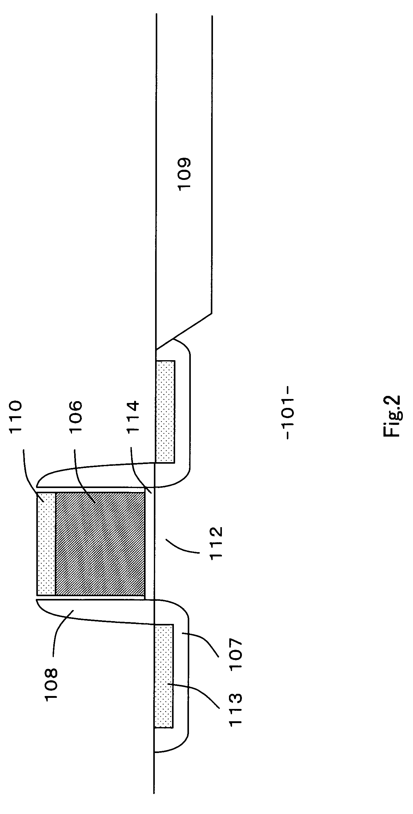
[0026]FIG. 1(A) is a cross sectional view low pressure taken along the line X-X′ of FIG. 1(B) vertical to the direction of extension of control gates 105 which act as word lines including active regions 111, illustrating a row of the memory cells arranged repeatedly a...


PUM


Abstract

According to the present invention, a method of manufacturing a semiconductor device which comprises a matrix of memory cells of the floating gate type is provided in which the silicon nitride layer is deposited as an etching stop layer on a control gate electrode for bottom borderless contact process with the threshold voltage of transistor arrangements being controlled not to change so that the productivity can remain not declined. In particular, the silicon nitride layer (115) is deposited as an etching stop layer on the control gate electrode (105) for bottom borderless contact process so that the concentration of hydrogen (H2) therein stays in a range from 1.5×10²¹ to 2.6×10²¹ atoms/cm3. Also, the silicon nitride layer (115) is deposited at a temperature of not higher than 700° C. by a low pressure CVD technique.

Description

CROSS REFERENCE TO RELATED APPLICATTION [0001] This Nonprovisional application claims priority under 35 U.S.C. §119(a) on Patent Application No. 2004-366473 filed in Japan on Dec. 17, 2004, the entire contents of which are hereby incorporated by reference. BACKGROUND OF THE INVENTION [0002] 1. Field of the Invention [0003] The present invention relates to a method of manufacturing a semiconductor device through a step of depositing a silicon nitride layer for bottom borderless contact process. [0004] 2. Description of the Related Art [0005] As large scale integrated circuit (LSI) devices become increasingly highly densified and integrated, a silicon nitride layer has been utilized as a diffusion layer for a contact hole opening in an upper inter-layer insulating layer or an etching stop layer over a self-aligned silicide layer, in order to bring the diffusion layer and the self-aligned silicide layer into contact with an upper wiring metal. [0006]FIG. 7 is a cross sectional view of ...

Claims


Application Information

Patent Timeline
Patent Type & Authority Applications(United States)
IPC IPC(8): H01L21/336H01L21/44
CPCH01L21/76897H01L27/115H01L27/11521H01L21/76834H10B69/00H10B41/30H01L21/18
Inventor INUZUKA, HIROYUKIDOI, TSUKASAMITSUMUNE, KAZUMASA
Owner SHARP KK
Why Eureka
Try Eureka