Semiconductor device, manufacturing method of the same and electronic device

Inactive Publication Date: 2006-06-29
RENESAS TECH CORP
View PDF5 Cites 11 Cited by
  • Summary
  • Abstract
  • Description
  • Claims
  • Application Information

AI Technical Summary

Benefits of technology

[0030] A semiconductor device equipped with an HBT which can satisfy both thermal stability and reliability and has improved electrostatic breakdown voltage can be provided.
[0031] An el

Problems solved by technology

The first problem is that the conventional technology, for example, the technology as d

Method used


Image

  • Semiconductor device, manufacturing method of the same and electronic device
  • Semiconductor device, manufacturing method of the same and electronic device
  • Semiconductor device, manufacturing method of the same and electronic device

Examples


embodiment 1

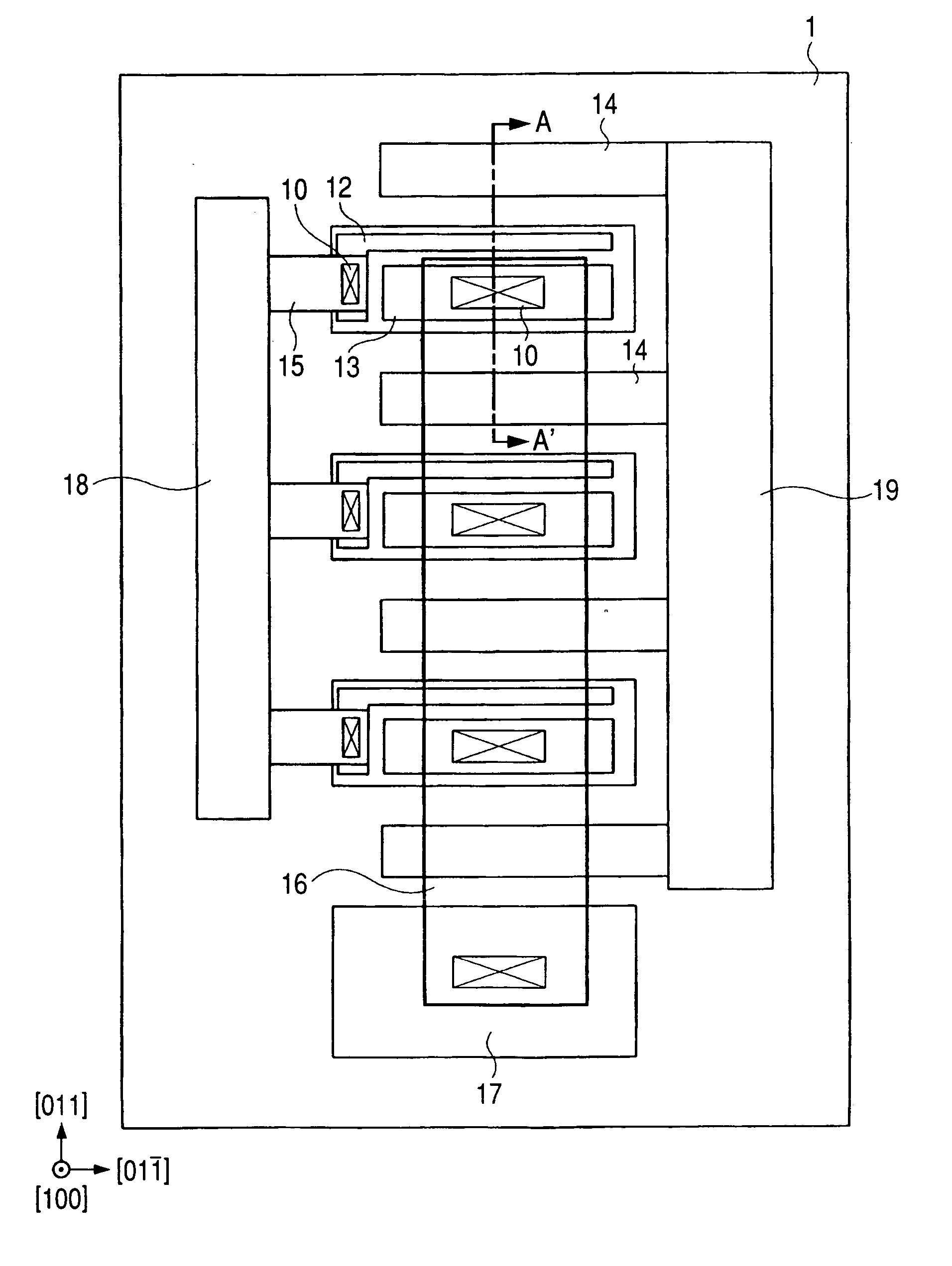
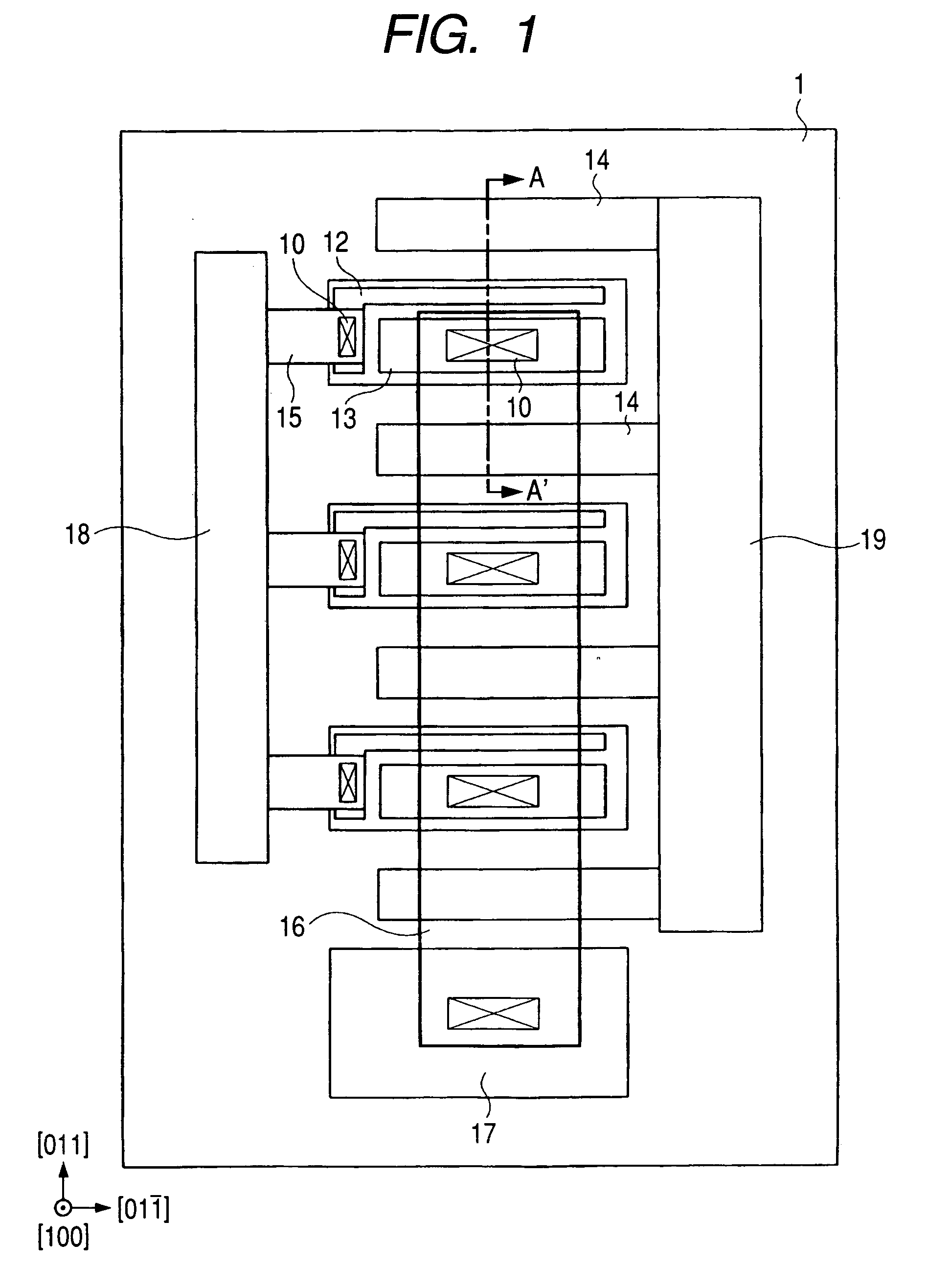
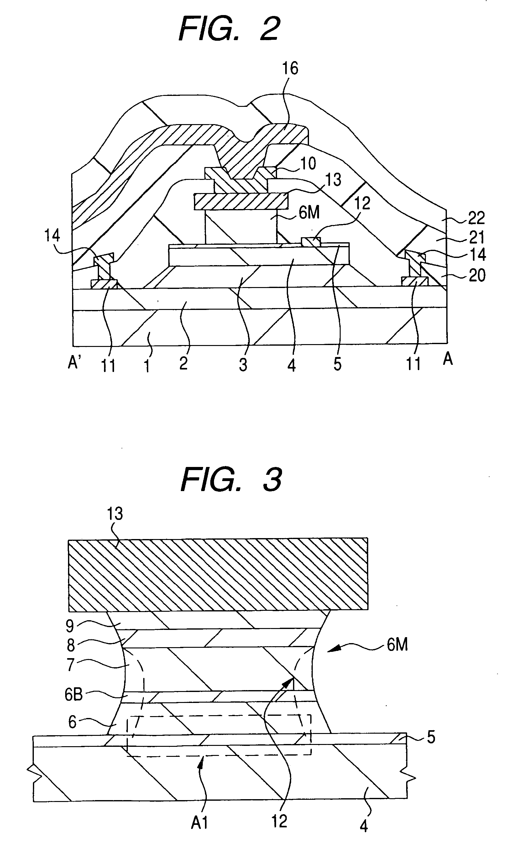
[0060] As one example of the semiconductor device according to the embodiment of the present invention, a semiconductor device equipped with a multifinger HBT for high power composed of a plurality of HBTs will next be described based on FIGS. 1 to 3. FIG. 1 is a schematic plan view of the semiconductor device, in which an emitter interconnect 16 is illustrated in perspective. FIG. 2 is a schematic cross-sectional view of the semiconductor device taken along a line A-A′ of FIG. 1. FIG. 3 is a fragmentary schematic cross-sectional view of the semiconductor device of FIG. 1. In this Embodiment, the semiconductor device is equipped with a plurality of HBTs, but it may be a semiconductor device equipped with one HBT. Incidentally, one HBT (which will hereinafter be called “basic HBT”) has an emitter area of 108 μm2.

[0061] A sub-collector layer (Si concentration: 5×1018 cm−3, film thickness: 0.6 μm) 2 made of, for example, an n type GaAs layer is formed over a substrate 1 made of a semi...

embodiment 2

[0092] In Embodiment 1, the ballast resistor layer is made of AlGaAs. In this Embodiment, a semiconductor device equipped with an HBT using a ballast resist layer made of AlGaInP or GaInAsP will be described as one example. The content of Embodiment 2 overlapped with that of Embodiment 1 is omitted from the description.

[0093] The semiconductor device according to this Embodiment is, as described using FIG. 2 in Embodiment 1, has an emitter layer 5 made of, for example, an n type InGaP layer, an emitter mesa layer 6M electrically connected to the emitter layer 5 and an emitter electrode 13 electrically connected to the emitter mesa layer 6M formed over a base layer 4 made of, for example, a p type GaAs layer.

[0094] As described above referring to FIG. 3 in Embodiment 1, this emitter mesa layer 6M has, over the emitter layer 5, a semiconductor layer 6 made of, for example, an n type GaAs layer, a high concentration semiconductor layer 6B made of, for example, an n+ type GaAs layer, ...

embodiment 3

[0098] In Embodiment 1, the emitter mesa layer 6M has both the ballast resistor layer 7 and high concentration semiconductor layer 6B therebelow. In this Embodiment, on the other hand, a semiconductor device equipped with an HBT having an emitter mesa layer 6M containing neither a ballast resistor layer 7 nor a high concentration semiconductor layer 6B, or an emitter mesa layer 6M not containing only the high concentration semiconductor layer 6B will be described as one example, based on FIGS. 14 to 18. The content of Embodiment 3 overlapped with that of Embodiment 1 is omitted from the description.

[0099]FIG. 14 is a fragmentary schematic cross-sectional view of the semiconductor device according to one example of this Embodiment. FIG. 15 is a schematic plan view of the semiconductor device according to the one embodiment during its manufacturing step. FIG. 16 is a fragmentary schematic cross-sectional view of the semiconductor device investigated by the present inventors. FIG. 17 ...


PUM


Abstract

Provided is a semiconductor device equipped with HBTs capable of satisfying both thermal stability and reliability and having improved electrostatic breakdown voltage.
The HBT according to the present invention is obtained by successively forming, over the main surface of a substrate made of a compound semiconductor, a sub-collector layer, a collector layer, a base layer, an emitter layer, a collector electrode electrically connected to the collector layer, a base electrode electrically connected to the base layer, an emitter mesa layer formed over the emitter layer and electrically connected to the emitter layer, and an emitter electrode electrically connected to the emitter mesa layer. The emitter mesa layer has a semiconductor layer made of an n type GaAs layer, a high concentration semiconductor layer made of an n+ type GaAs layer over the semiconductor layer and a ballast resistor layer made of an n type InGaAs layer over the high concentration semiconductor layer.

Description

CROSS-REFERENCE TO RELATED APPLICATION [0001] The present application claims priority from Japanese patent application No. 2004-375632 filed on Dec. 27, 2004, the content of which is hereby incorporated by reference into this application. BACKGROUND OF THE INVENTION [0002] The present invention relates to a semiconductor device and a manufacturing technology thereof, in particular, to a technology effective when applied to a hetero-junction bipolar transistor (which will hereinafter be abbreviated as “HBT”). Further, the present invention pertains to an electronic device using it. [0003] In recent years, with rapid growth of demand of wireless communications equipment, research and development on a power amplifier used for the communications equipment has been carried out intensively. Examples of semiconductor transistors used for a power amplifier for mobile communications equipment include HBT, field effect transistor and silicon (Si)-MOSFET (Metal Oxide Semiconductor Field Effect...

Claims


Application Information

Patent Timeline
IPC IPC(8): H01L31/109
CPCH01L29/41708H01L29/42304H01L29/7304H01L29/7371
Inventor KUROKAWA, ATSUSHIOHBU, ISAOUMEMOTO, YASUNARISASAKI, SATOSHIKUSANO, CHUSHIROIMAMURA, YOSHINORI
Owner RENESAS TECH CORP
Why Eureka
Try Eureka