Method for manufacturing PMOSFET

a manufacturing method and technology of pmosfet, applied in the direction of basic electric elements, electrical apparatus, semiconductor devices, etc., can solve the problems of threshold voltage shift and off-current increase, difficult channel control, surface channel-type pmosfet to be used in memory devices, etc., to improve the characteristics and reliability of pmosfet transistors, stable threshold voltage, and reduced channel dose

Inactive Publication Date: 2006-06-29
SK HYNIX INC
View PDF3 Cites 9 Cited by
  • Summary
  • Abstract
  • Description
  • Claims
  • Application Information

AI Technical Summary

Benefits of technology

[0008] Accordingly, the present invention has been made to solve the above-mentioned problems occurring in the prior art, and an object of the present invention is to provide a method for manufacturing a PMOSFET using a trench-type gate structure only in a PMOSFET r

Problems solved by technology

In the case of an embedded channel-type PMOSFET, the channel control becomes more difficult, as the device size decreases, due to degradation of threshold voltage and leak current characteristics, which are fundamental problems of the embedded channel.
A surface channel-type PMOSFET is difficult to be used in a memory device, because the fundamental problem of boron intrusion has not yet been solved.
In t

Method used


Image

  • Method for manufacturing PMOSFET
  • Method for manufacturing PMOSFET
  • Method for manufacturing PMOSFET

Examples


Embodiment Construction

[0021] Hereinafter, a preferred embodiment of the present invention will be described with reference to the accompanying drawings. In the following description and drawings, the same reference numerals are used to designate the same or similar components, and so repetition of the description on the same or similar components will be omitted.

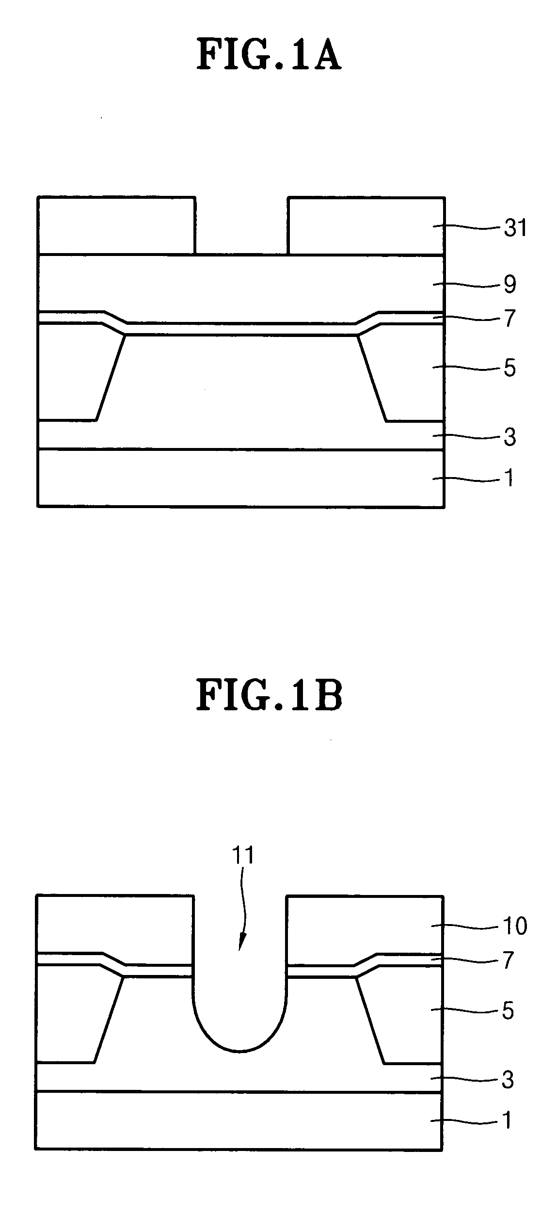
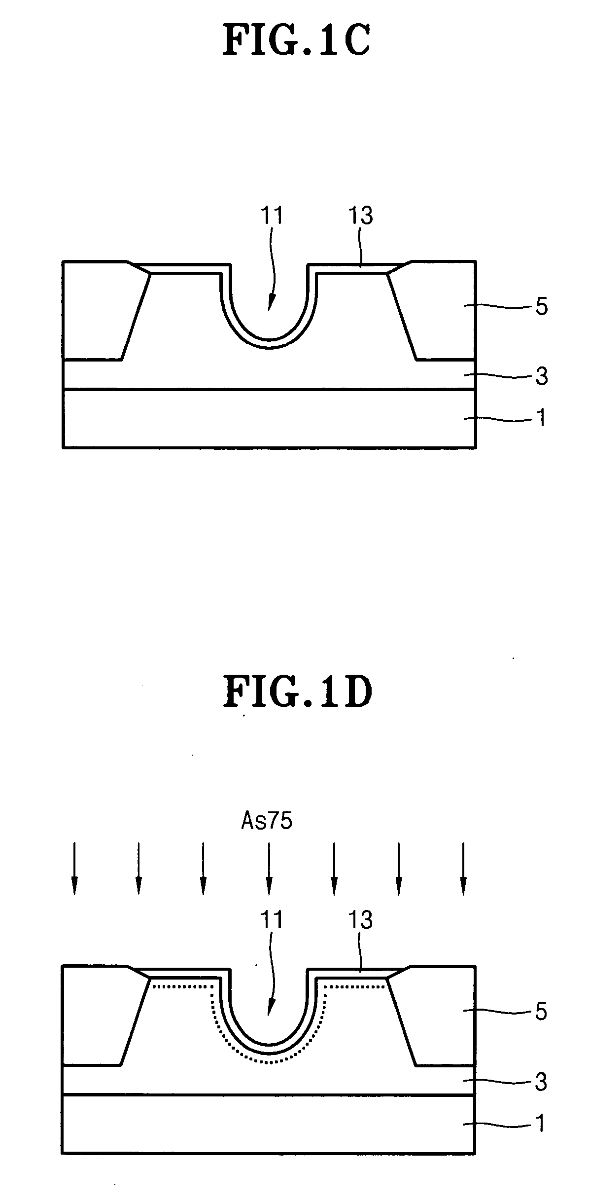
[0022]FIGS. 1A to 1I are sectional views showing processes of a method for manufacturing a PMOSFET according to the present invention.

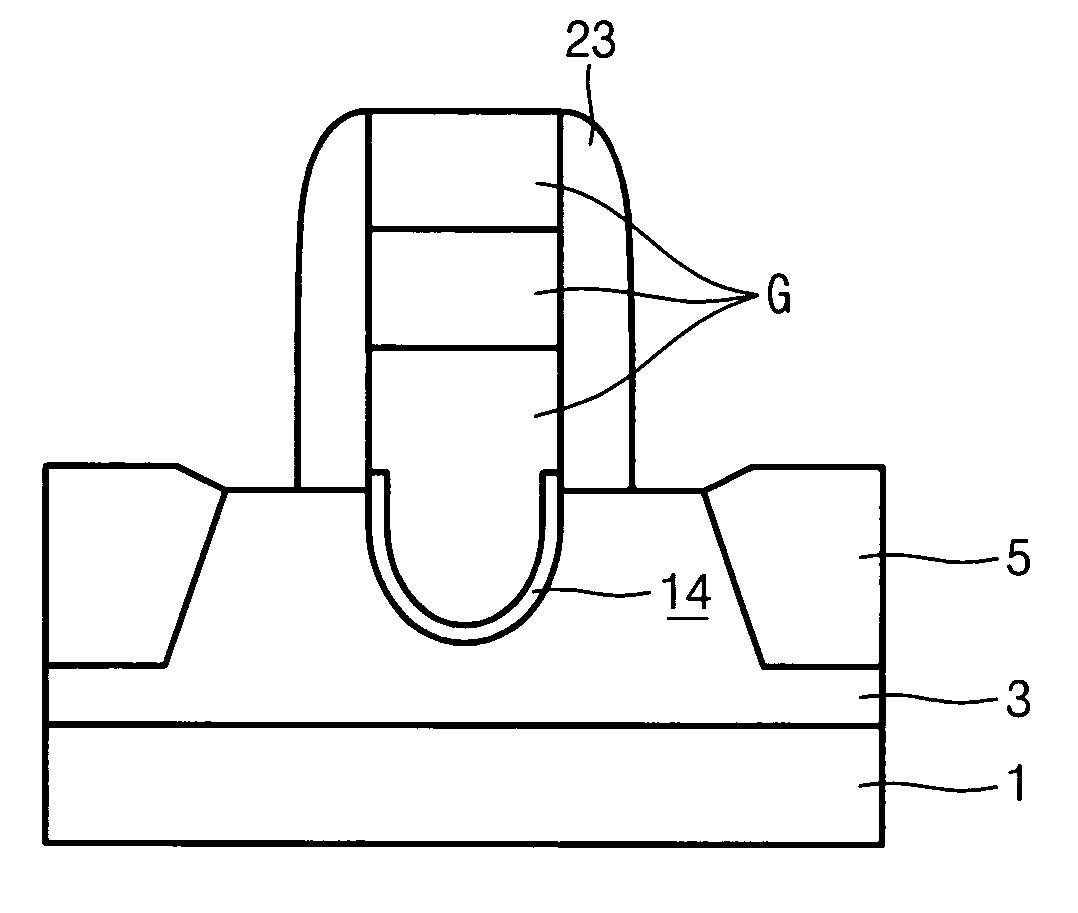
[0023] In a method for manufacturing a PMOSFET according to the present invention, as shown in FIG. 1A, a semiconductor substrate 1 having a PMOS region of a peripheral circuit defined thereon is provided. An isolation layer 5 is formed on the substrate 1 in a conventional STI (shallow trench isolation) process and an N well 3 is formed thereon through implantation for well formation. A pad oxide film 7, a hard mask polycrystalline silicon film 9, and a first photoresist pattern 31 for exposing a gate formation r...


PUM


Abstract

A method for manufacturing a PMOSFET uses a trench-type gate structure only in a PMOSFET region of a peripheral circuit, except for a cell, to overcome the shortcomings of a MOSFET caused by reduction in design rule, realize stable threshold voltage, and improve the characteristics and reliability of a PMOSFET transistor through reduction in channel dose.

Description

BACKGROUND OF THE INVENTION [0001] 1. Field of the Invention [0002] The present invention relates to a method for manufacturing a PMOSFET, and more particularly to a method for manufacturing a PMOSFET using a trench-type gate structure only in a PMOSFET region of a peripheral circuit, except for a cell, to reduce the area of the peripheral circuit and improve the production yield rate. [0003] 2. Description of the Prior Art [0004] As generally known in the art, a PMOSFET may be classified into a surface channel type and an embedded channel type. In the case of an embedded channel-type PMOSFET, the channel control becomes more difficult, as the device size decreases, due to degradation of threshold voltage and leak current characteristics, which are fundamental problems of the embedded channel. [0005] A surface channel-type PMOSFET is difficult to be used in a memory device, because the fundamental problem of boron intrusion has not yet been solved. When a p-type gate is formed on a ...

Claims


Application Information

Patent Timeline
IPC IPC(8): H01L21/336
CPCH01L29/4236H01L29/66621H01L29/78H01L29/7835H01L21/18H01L21/32H01L21/28H01L21/265
Inventor CHUN, YUN SEOK
Owner SK HYNIX INC
Why Eureka
Try Eureka