CMOS image sensor and method for fabricating the same

a technology of image sensor and cmos, which is applied in the direction of diodes, radiation control devices, semiconductor devices, etc., can solve the problems of difficult to ensure the isolation characteristics of photodiodes, the limit of ensuring isolation characteristics between pixels and plugs, and the difficulty of ensuring isolation characteristics between photodiodes, etc., to achieve the effect of improving reflection characteristics

Active Publication Date: 2006-07-06
DONGBU HITEK CO LTD
View PDF4 Cites 14 Cited by
  • Summary
  • Abstract
  • Description
  • Claims
  • Application Information

AI Technical Summary

Benefits of technology

[0015] An advantage of the present invention is to provide a CMOS image sensor and a method for fabricating the same in which light-shielding layers are formed between micro lenses to improve reflection characteristics and to protect the micro lenses upon packaging
[0016] Additional features and advantages of the invention will be set forth in the description which follows, and in part will be apparent from the description, or may be learned by practice of the invention. The objectives and other advantages of the invention will be realized and attained by the structure and method particularly pointed out in the written description and claims hereof as well as the appended drawings.
[0017] To achieve these and other advantages and in accordance with the purpose of the present invention, as embodied and broadly described, a CMOS image sensor includes a semiconductor substrate including a first epitaxial layer, a first photodiode formed on the semiconductor substrate including the first epitaxial layer, a second epitaxial layer formed on the semiconductor substrate including the first photodiode, a plurality of device isolation layers formed in isolation regions, wherein the isolation regions are formed at the second epitaxial layer, a second photodiode formed in the second epitaxial layer between the device isolation layers, and a third epitaxial layer formed on the second epitaxial layer including the second photodiode.
[0018] In another aspect of the present invention, the third epitaxial layer is selectively grown on the second epitaxial layer except the device isolation layers.
[0019] In another aspect of the present invention, the CMOS image sensor further includes a first plug formed on the semiconductor substrate for extracting a signal from the first photodiode, and a second plug formed on the semiconductor substrate for extracting a signal from the second photodiode.
[0020] In another aspect of the present invention, the first plug is formed from the semiconductor substrate at a side of the first photodiode to the second epitaxial layer and the second plug is formed in the third epitaxial layer.

Problems solved by technology

Since a diffusion layer is used when the photodiode is formed, there is a limit in ensuring isolation characteristics between pixels and between a plug unrelated to the pixel and the photodiode.
Also, since the photodiode is formed below the STI region, it is difficult to ensure isolation characteristics between the photodiodes.

Method used


Image

  • CMOS image sensor and method for fabricating the same
  • CMOS image sensor and method for fabricating the same
  • CMOS image sensor and method for fabricating the same

Examples


Embodiment Construction

[0032] Reference will now be made in detail to exemplary embodiments of the present invention, examples of which are illustrated in the accompanying drawings. Wherever possible, the same reference numbers will be used throughout the drawings to refer to the same or similar parts.

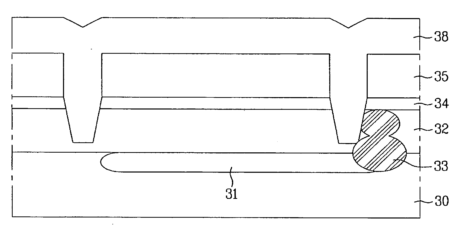
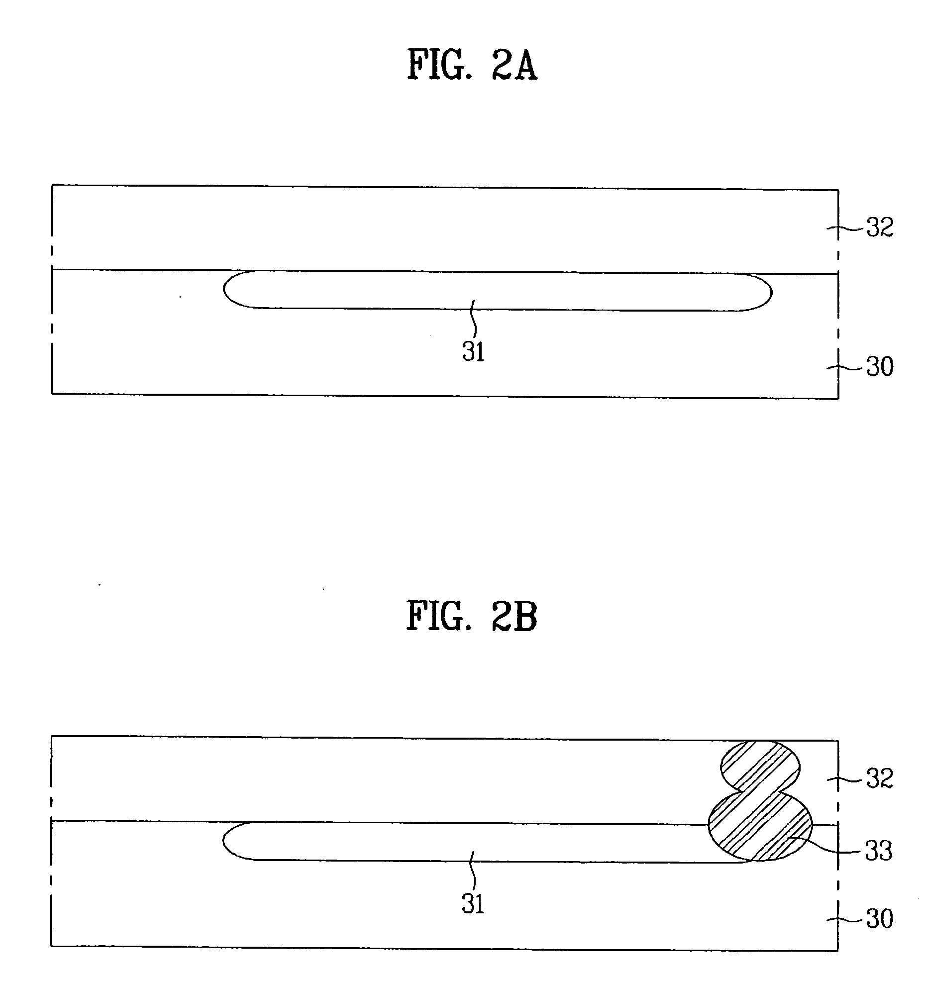
[0033] As illustrated in FIG. 2A, boron ions are injected into an entire surface of a semiconductor substrate 30 in which a first epitaxial layer (not shown) is grown. Then, a first photoresist (not shown) is coated on the semiconductor substrate 30 and partially etched to form a first photoresist pattern (not shown) which exposes a red photodiode region. Arsenic ions are injected into the first epitaxial layer to form a red photodiode 31 and then the first photoresist pattern is removed. Then, a second epitaxial layer 32 is grown on the semiconductor substrate 30 including the red photodiode 31 at a predetermined thickness.

[0034] As illustrated in FIG. 2B, in order to form a first plug connected to the re...


PUM


Abstract

A CMOS image sensor and a method for fabricating the same can ensure isolation characteristics using a shallow trench isolation (STI) process and a selective epitaxy method. The CMOS image sensor and method for fabricating the same can also reduce pixel size. The CMOS image sensor includes a semiconductor substrate, a first photodiode, a first epitaxial layer, a second epitaxial layer, a plurality of device isolation layers formed in isolation regions formed at the second epitaxial layer, a second photodiode formed between the device isolation layers, and a third epitaxial layer.

Description

[0001] This application claims the benefit of Korean Patent Application No. 10-2004-0116427, filed on Dec. 30, 2004, which is hereby incorporated by reference for all purposes as if fully set forth herein. BACKGROUND OF THE INVENTION [0002] 1. Field of the Invention [0003] The present invention relates to a CMOS image sensor and a method for fabricating the same. More particularly, the present invention relates to a vertical CMOS image sensor and a method for fabricating the same, which can reduce pixel size and can ensure isolation characteristics using a shallow trench isolation (STI) process and a selective epitaxy method. [0004] 2. Discussion of the Related Art [0005] Generally, an image sensor is a semiconductor device that converts an optical image to an electric signal. In a CCD (charge coupled device) image sensor, a plurality of MOS (metal-oxide-metal) capacitors are arranged close to one another to transfer and store electric charge carriers. In a CMOS (complementary MOS) ...

Claims


Application Information

Patent Timeline
Patent Type & Authority Applications(United States)
IPC IPC(8): H01L31/062H01L31/113H01L29/768
CPCH01L27/14627H01L27/1463H01L27/14643H01L27/14645H01L27/14647H01L27/14685H01L27/14689H01L27/146H01L31/10
Inventor LEE, SANG GI
Owner DONGBU HITEK CO LTD
Why Eureka
Try Eureka