CMOS active pixel sensor with improved dynamic range and method of operation

a pixel sensor and active technology, applied in the field of solid-state electronic image sensors, can solve the problems of high volume commercial grade cmos imaging products, sensor characteristics close to those of ccd, and high cost and complexity of silicon ccd manufacturing processes

Active Publication Date: 2006-07-06
THE BF GOODRICH CO
View PDF15 Cites 84 Cited by
  • Summary
  • Abstract
  • Description
  • Claims
  • Application Information

AI Technical Summary

Benefits of technology

[0047] The present invention is unique compared to prior art since it provides a CMOS APS pixel incorporating two distinct and differently performing amplifier circuits within each pixel, and that each pixel can stand alone as an individually accessible detector element in a larger array of detector elements.

Problems solved by technology

The processes related to silicon CCD manufacturing have always been reasonably expensive and complex, with the implementation technology of choice being N type metal oxide (NMOS).
Today, CMOS imager development has yielded a sensor with characteristics close to that of the CCD, but still lacking in some respects.
Few, if any, high volume commercial grade CMOS imaging products are manufactured using uniquely customized image sensor specific processes or complex pixel design technologies.
Although some CMOS imager foundries have begun to support unique process modifications to create specific process and design features for application specific integrated circuit (ASIC) clients, in nearly every case the custom CMOS image sensor technologies that enable these high performance applications are unique to the ASIC client, and not accessible to other users.
However, as airborne reconnaissance systems begin to incorporate additional functionality and interoperability through reductions in size, weight, power, and cost, it is becoming increasingly difficult for CCD technology to support these objectives, due to limitations in the fundamental fabrication and operational principles of the CCD image sensor itself.
Although present CMOS image sensor technology does not support the broad, demanding performance requirements currently provided by the CCD, the successful evolution of airborne reconnaissance imaging systems will rely on the adaptation of CMOS image sensor technology to enable the improvements necessary to advance the art.
The prior art methods to extend detector dynamic range do not preserve the linear response of the detector while maintaining signal integrity for both high and low scene illumination levels.
The full well capacity of a CCD image sensor pixel is generally limited by the charge handling capacity of a gated potential well that usually has an antiblooming feature to avoid signal charge from mixing with adjacent pixels when a pixel that has reached its well saturation limit.
Conversely, the saturation limit of a CMOS image sensor is typically more a complex function of the floating diffusion sense node voltage swing, photodiode storage capacity, and additional capacitances added to the pixel amplifier circuit.
Unfortunately, the maximum voltage swing is limited by the maximum allowable Vdd voltage for the CMOS process design rules being used.
As previously stated, this creates a conflict for conventional pixel design.

Method used


Image

  • CMOS active pixel sensor with improved dynamic range and method of operation
  • CMOS active pixel sensor with improved dynamic range and method of operation
  • CMOS active pixel sensor with improved dynamic range and method of operation

Examples


Embodiment Construction

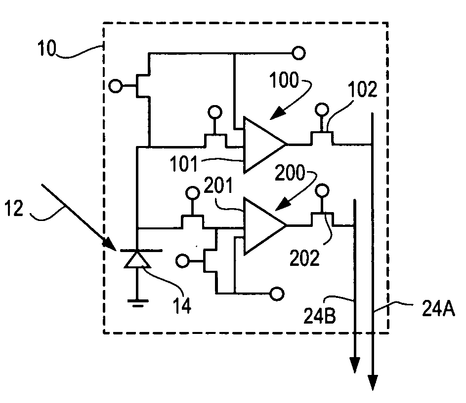
[0066] In a first aspect, an improved CMOS imaging array is provided comprising a plurality of individual pixels arranged in an array of rows and columns of individual pixels. The number of pixels can vary, but embodiments of 25 and 50 million pixels are considered exemplary. Each pixel in the plurality of individual pixel sensors is preferably the same. A representative example of the CMOS pixel sensor 10 is shown in FIG. 5A. The pixel sensor includes the following elements:

[0067] a) A photodetector 14 receiving incident light 12 and generating an output (accumulated charge).

[0068] b) A first relatively lower gain, wide dynamic range amplifier circuit 100 responsive to the output of the photodetector 14, the first circuit 100 optimized for a linear response to high light level input signals. The amplifier circuit 100 may also function as a charge to voltage conversion circuit.

[0069] c) A second relatively higher gain, lower dynamic range amplifier circuit 200 responsive to the o...


PUM


Abstract

A CMOS imaging array includes a plurality of individual pixels arranged in rows and columns. Each pixel is constructed the same and includes a photodetector (e.g., photodiode) receiving incident light and generating an output. A first, relatively lower gain, wide dynamic range amplifier circuit is provided responsive to the output of the photodetector. The first circuit is optimized for a linear response to high light level input signals. A second, relatively higher gain, lower dynamic range amplifier circuit is also provided which is responsive to the output of the photodetector. The second circuit is optimized to provide a high signal to noise ratio for low light level input signals. A first output select circuit is provided for directing the output of the first circuit to a first output multiplexer. A second output select circuit is provided for directing the output of the second circuit to a second output multiplexer. Thus, separate outputs of the first and second circuits are provided for each of the individual pixel sensors of the CMOS imaging array. Alternative embodiments incorporate two ore more photodetectors and two or more amplifier circuits and output select circuits. Three photodetectors and three amplifier circuits are useful for an embodiment where the sensor includes a three-color filter matrix.

Description

BACKGROUND OF THE INVENTION [0001] A. Field of the Invention [0002] The present invention relates to solid state electronic image sensors and in particular to a Complementary Metal Oxide Semiconductor (CMOS) array with a pixel design which improves the operational dynamic range of the sensor. It is particularly suitable for application to airborne imaging systems, such as military aerial reconnaissance image sensors. [0003] B. Description of Related Art [0004] Image sensors for capturing electronic representations of images in the visible wavelengths have been around since about 1970, when the silicon charge coupled device (CCD) was invented. Over the years, CCDs have become the standard for visible spectrum electronic imaging, replacing film in most applications. Various architectures have been developed to make CCD operation more effective for the specific application. Such architectures include the full frame, frame transfer, and interline transfer CCD. [0005] The processes relat...

Claims


Application Information

Patent Timeline
Patent Type & Authority Applications(United States)
IPC IPC(8): H04N5/335H04N5/355
CPCH01L27/14603H01L27/14609H01L27/14621H01L27/14689H04N5/35545H04N5/35563H04N5/3559H04N5/374H04N5/3745H04N25/581H04N25/585H04N25/59H04N25/76H04N25/77
Inventor FARRIER, MICHAEL
Owner THE BF GOODRICH CO
Why Eureka
Try Eureka