Epoxy resin composition and semiconductor device

a technology of epoxy resin and semiconductors, applied in the directions of semiconductor/solid-state device details, synthetic resin layered products, transportation and packaging, etc., can solve the problems of undesirable use of these compounds, inability to solve the conventional epoxy resin composition, and increasing the demand for epoxy resin compositions for semiconductor encapsulation. , to achieve the effect of excellent flowability and solder crack resistan

Inactive Publication Date: 2006-07-13
SUMITOMO BAKELITE CO LTD
View PDF0 Cites 6 Cited by
  • Summary
  • Abstract
  • Description
  • Claims
  • Application Information

AI Technical Summary

Benefits of technology

[0006] The object of the present invention is to provide an epoxy resin composition for semiconductor encapsulation which is excellent in flowability and solder crack resistance, and a semiconductor device obtained using the composition.

Problems solved by technology

Moreover, the area mounting of semiconductor devices is being facilitated, and, consequently, demand for epoxy resin compositions for semiconductor encapsulation becomes increasingly severer.
Therefore, there are problems which cannot be solved by the conventional epoxy resin compositions.
Usually, bromine-containing organic compounds and antimony compounds such as antimony trioxide and antimony tetroxide are added to epoxy resin compositions in order to impart flame retardancy to the compositions, but use of these compounds is undesirable from the environmental and hygienic points.
However, the resins having many aromatic rings have the defect of increase of viscosity.
The solder crack resistance can be considerably improved by employing the above method, but there is a problem that with increase of the filling ratio of the inorganic filler, the flowability is sacrificed and vacant voids are apt to be produced in the package.
However, delamination at the interface of cured epoxy resin composition and each bonded portion subjected to various platings such as gold plating or silver plating cannot be prevented, and an epoxy resin composition for semiconductor encapsulation which has a sufficiently satisfactory solder crack resistance cannot still be obtained.

Method used


Image

  • Epoxy resin composition and semiconductor device
  • Epoxy resin composition and semiconductor device
  • Epoxy resin composition and semiconductor device

Examples


example 1

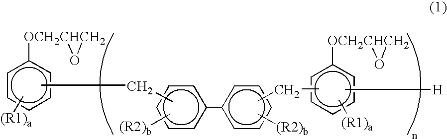
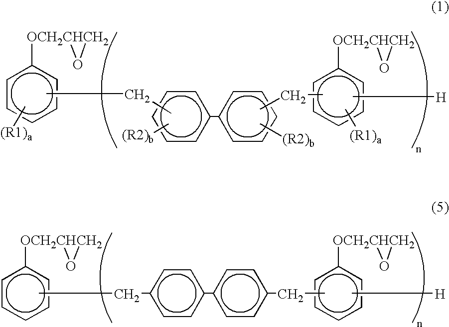
[0037] Epoxy resin 1: An epoxy resin represented by the following formula (5) (NC3000P manufactured by Nippon Kayaku Co., Ltd. and having a softening point of 58° C. and an epoxy equivalent of 273, which is hereinafter referred to as “E-1”) [0038] - - - 49 parts by weight

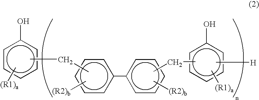
[0039] Phenolic resin 1: A phenolic resin represented by the following formula (6) (MEH-7851SS manufactured by Meiwa Kasei Co., Ltd. and having a softening point of 107° C. and a hydroxyl equivalent of 204, which is hereinafter referred to as “H-1”) [0040] - - - 42 parts by weight

[0041] 1,8-Diazabicyclo(5,4,0)undecene-7 (hereinafter referred to as “DBU”)

[0042] - - - 5 parts by weight

Fused spherical silica (average particle870 parts by weightdiameter 21 μm)Coupling agent 1 3 parts by weightCoupling agent 2 3 parts by weightCarbon black 3 parts by weightCarnauba wax 5 parts by weight

[0043] The above components were mixed by a mixer, and the mixture was kneaded at 95° C. for 8 minutes using a hot roll, cooled an...


PUM

PropertyMeasurementUnit
temperatureaaaaaaaaaa
melting pointaaaaaaaaaa
temperatureaaaaaaaaaa

Abstract

The object of the present invention is to provide an epoxy resin composition for semiconductor encapsulation which is excellent in flowability, adhesion to substrates, flame retardancy and solder crack resistance without using bromine-containing organic compounds and antimony compounds. According to the present invention, there is provided an epoxy resin composition for semiconductor encapsulation characterized by including, as essential components, a phenolic aralkyl type epoxy resin having a biphenyl structure, a phenolic aralkyl resin having a biphenyl structure, a curing accelerator, an inorganic filler, a specific silane coupling agent having a secondary amine, and a specific silane coupling agent having a mercapto group.

Description

TECHNICAL FIELD [0001] The present invention relates to an epoxy resin composition for encapsulation of semiconductors, and a semiconductor device obtained using the composition. BACKGROUND OF THE INVENTION [0002] As a method for encapsulation of semiconductor elements such as IC and LSI, the transfer molding of an epoxy resin composition has been employed for a long time because it is low in cost and suitable for mass-production. Further, as for the reliability, improvement of characteristics has been attempted by amelioration of epoxy resins or phenolic resins as curing agents. However, high integration of semiconductors has advanced year by year in accordance with the recent market demand for miniaturization, weight-saving and high-performance of electronic equipment. Moreover, the area mounting of semiconductor devices is being facilitated, and, consequently, demand for epoxy resin compositions for semiconductor encapsulation becomes increasingly severer. Therefore, there are pr...

Claims


Application Information

Patent Timeline
Patent Type & Authority Applications(United States)
IPC IPC(8): B32B27/38C08L63/00H01L21/56B32B37/00
CPCC08G59/245C08G59/3218C08L63/00H01L23/293H01L2924/0002H01L2924/12044H01L2924/00Y10T428/31511
Inventor NISHIKAWA, ATSUNORI
Owner SUMITOMO BAKELITE CO LTD
Why Eureka
Try Eureka