
Method for fabricating low-defect-density changed orientation Si

a technology of density and orientation, applied in semiconductor/solid-state device manufacturing, basic electric elements, electric devices, etc., can solve the problems of short time in the absence of dopants, damage layer interferes with the clean recrystallization of amorphized, and short time is not optimal for defect removal

Inactive Publication Date: 2006-07-13
GLOBALFOUNDRIES INC
View PDF4 Cites 41 Cited by
  • Summary
  • Abstract
  • Description
  • Claims
  • Application Information

AI Technical Summary

Benefits of technology

[0013] A related object of the present invention is to provide an ATR method for changing the orientation of selected regions of silicon without leaving a large density of defects.

Problems solved by technology

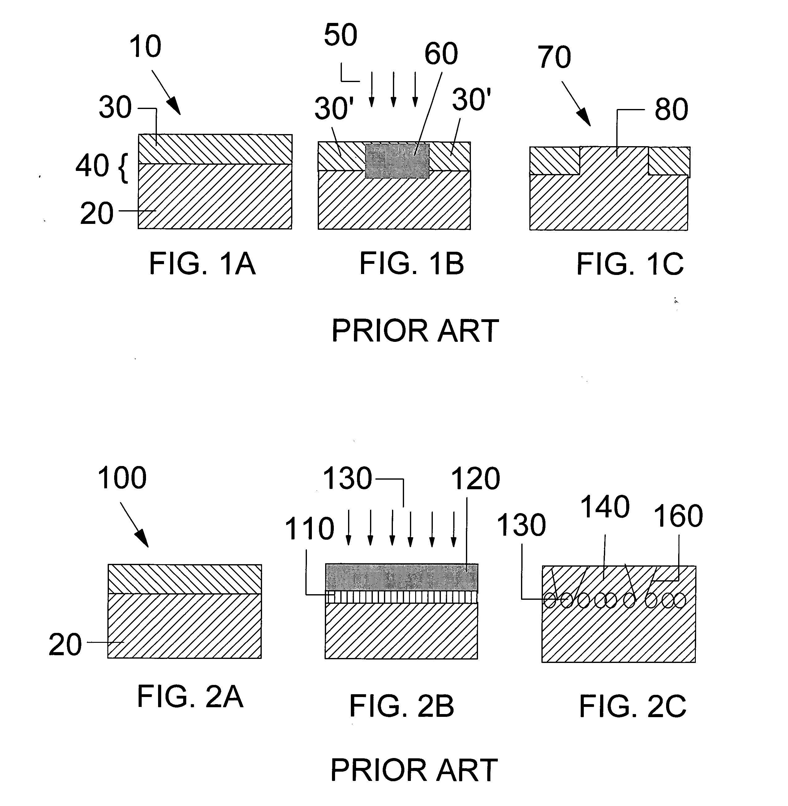
The damage layer interferes with the clean recrystallization of the amorphized Si, both by introducing threading defects (which can propagate to the wafer's surface) and by leaving a band of dislocation loops at the approximate position of the original damage layer.
However these short times are not optimal for defect removal in the absence of dopants (e.g., when amorphization is effected by implantation of Si+ or Ge+).

Method used


Image

  • Method for fabricating low-defect-density changed orientation Si
  • Method for fabricating low-defect-density changed orientation Si
  • Method for fabricating low-defect-density changed orientation Si

Examples


examples

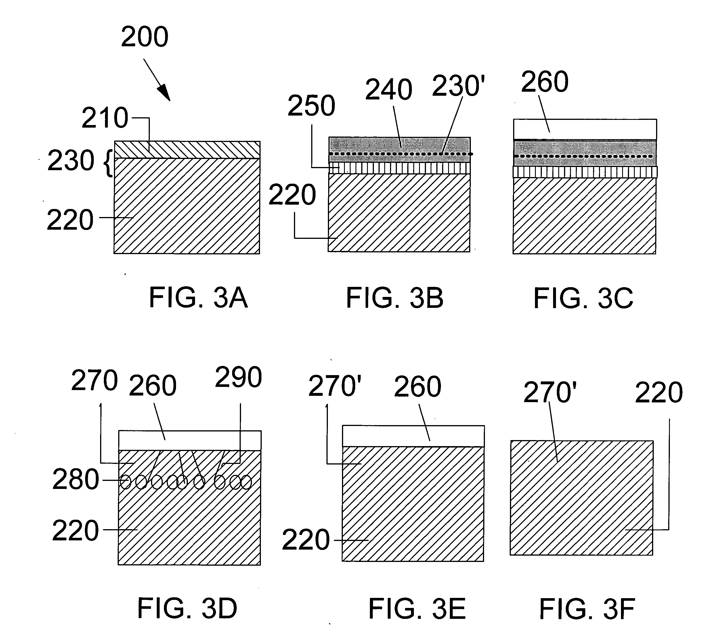
[0049] The steps of an exemplary anneal for the Si recrystallization process of this invention are listed below. [0050] Ramp up from 250° C. to 650° C. at 5° C. / min in Ar+[0051] 650° C. / 30 min in Ar+[0052] Ramp up from 650° C. to 1000° C. at 5° C. / min in Ar+[0053] Ramp up from 1000° C. to 1150° C. at 2° C. / min in Ar / O2(0.63%)+[0054] Ramp up from 1150° C. to 1310° C. at 1° C. / min in Ar / O2(0.63%)+[0055] Ramp up from 1310° C. to 1320° C. at 0.5° C. / min in Ar / O2(1.2%)+[0056] 1320° C. / 3 h in Ar / O2(1.2%)+[0057] Ramp down from 1320° C. to 1150° C. at −2° C. / min in Ar / O2(0.63%)+[0058] Ramp down to 400° C. at −5° C. / min in N2.

The 650° C. / 30 min Ar anneal may be viewed as the initial recrystallization anneal, while the 1320° C. / 3 hr anneal in Ar / O2 may be viewed as the defect removal anneal. Without a protective cap layer, this anneal would typically produce 90-110 nm of SiO2, corresponding to the consumption of about 50 nm of Si. With a protective cap layer of 100 nm SiO2, additional oxide...


PUM

PropertyMeasurementUnit
temperatureaaaaaaaaaa
temperaturesaaaaaaaaaa

Abstract

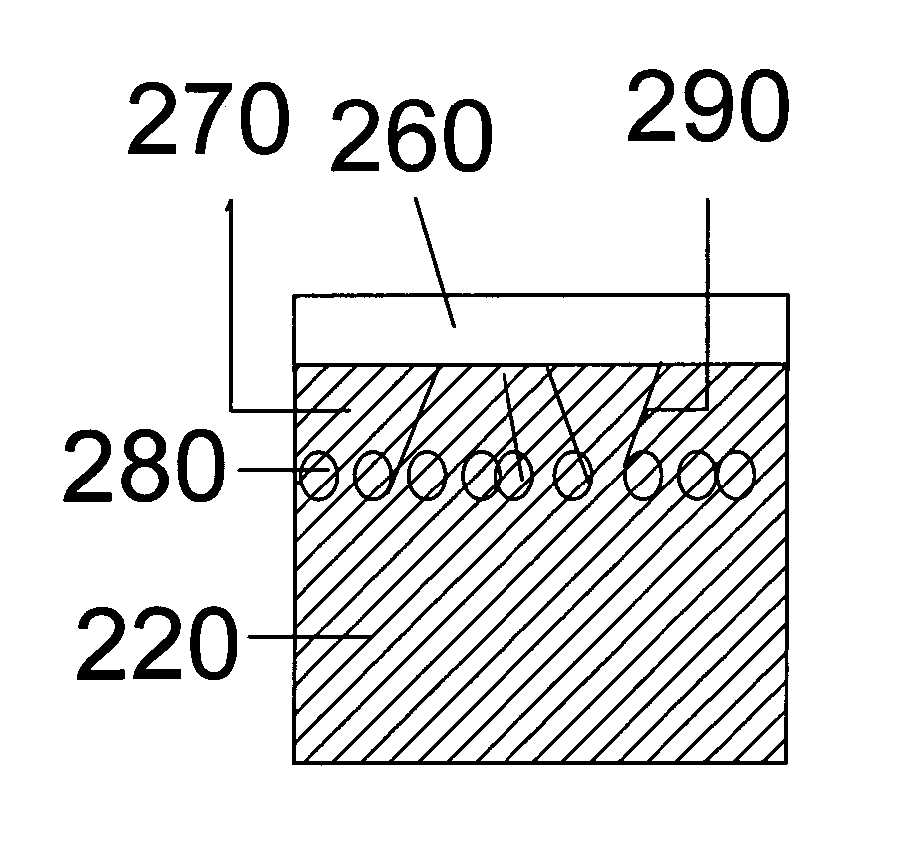
The present invention provides a method for forming low-defect density changed-orientation Si by amorphization / templated recrystallization (ATR) processes in which regions of Si having a first crystal orientation are amorphized by ion implantation and then recrystallized into the orientation of a template layer having a different orientation. More generally, the invention relates to the high temperature annealing conditions needed to eliminate the defects remaining in Si-containing single crystal semiconductor materials formed by ion-implant-induced amorphization and templated recrystallization from a layer whose orientation may be the same or different from the amorphous layer's original orientation. The key component of the inventive method is a thermal treatment for minutes to hours in the the temperature range 1250-1330° C. to remove the defects remaining after the initial recrystallization anneal. The invention also provides a low-defect density changed-orientation Si formed by ATR for use in hybrid orientation substrates.

Description

CROSS REFERENCE TO RELATED APPLICATION [0001] This application relates to cofiled U.S. application Ser. No. ______ (Attorney Docket YOR920040435US1) filed on Jan. 7, 2005, entitled “Quasi-hydrophobic Si—Si wafer bonding using hydrophilic Si surfaces and dissolution of interfacial bonding oxide” which is incorporated herein by reference.FIELD OF THE INVENTION [0002] The present invention relates to the formation of low-defect density changed-orientation Si by amorphization / templated recrystallization (ATR) processes in which regions of Si having a first crystal orientation are amorphized by ion implantation and then recrystallized into the orientation of a template layer having a different orientation. More generally, the invention relates to the high temperature annealing conditions needed to eliminate the defects remaining in Si-containing single crystal semiconductor materials formed by ion-implant-induced amorphization and templated recrystallization from a layer whose orientatio...

Claims


Application Information

Patent Timeline
Patent Type & Authority Applications(United States)
IPC IPC(8): H01L21/336
CPCH01L21/2022H01L21/26506H01L21/02667H01L21/02598H01L21/02532H01L21/02529H01L21/02609H01L21/02378H01L21/02381H01L21/02694H01L21/02672H01L21/02433
Inventor DE SOUZA, JOEL PEREIRAFOGEL, KEITH EDWARDOTT, JOHN ALBRECHTSADANA, DEVENDRA KUMARSAENGER, KATHERINE LYNN
Owner GLOBALFOUNDRIES INC
Learn More